Moisture sensor arrangement

a moisture sensor and arrangement technology, applied in the field of moisture sensor arrangement, can solve the problem that the overall construction of the sensor arrangement requires two semiconductors, and achieve the effect of achieving the invention, and reducing the size of the structur

Active Publication Date: 2017-12-19
E E ELEKTRONIK GES
View PDF26 Cites 1 Cited by
  • Summary
  • Abstract
  • Description
  • Claims
  • Application Information

AI Technical Summary

Benefits of technology

[0008]An object of the present invention is to disclose a moisture sensor arrangement of compact structure that is simple to contact electrically and by way of which reliable measurement of the ambient moisture is possible.
[0027]One resultant advantage of the moisture sensor arrangement of the present invention is an extremely compact structure. The electrical contacting of the moisture sensor arrangement requires no bond wires, and thus the space the signal processing component requires is reduced to its own external dimensions. An additional housing for protecting the bond wires can be dispensed with as well, which also proves favorable with regard to requiring only little space. Moreover, nearly the entire surface area of the signal processing component can be used for the moisture sensor, and as a result, greater precision of the moisture sensor arrangement of the present invention can be attained.

Problems solved by technology

A disadvantage of this version is that the overall construction of the sensor arrangement requires two semiconductor substrates.

Method used


Image

  • Moisture sensor arrangement
  • Moisture sensor arrangement
  • Moisture sensor arrangement

Examples


Embodiment Construction

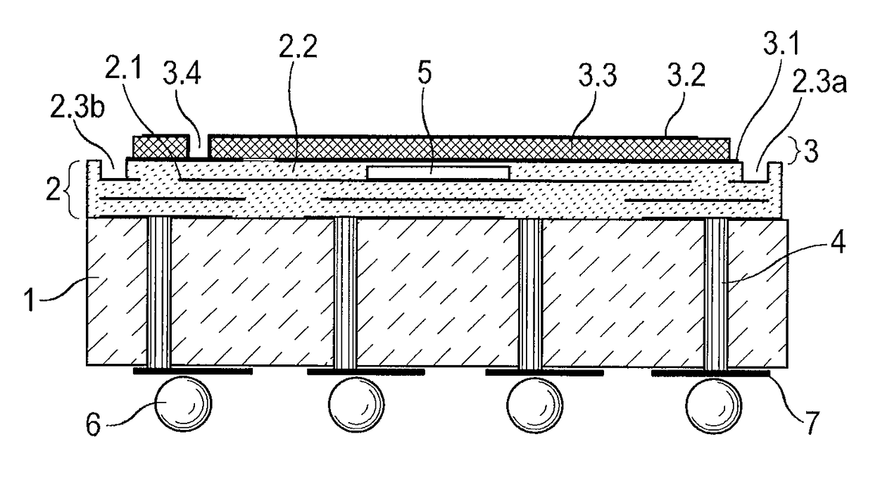
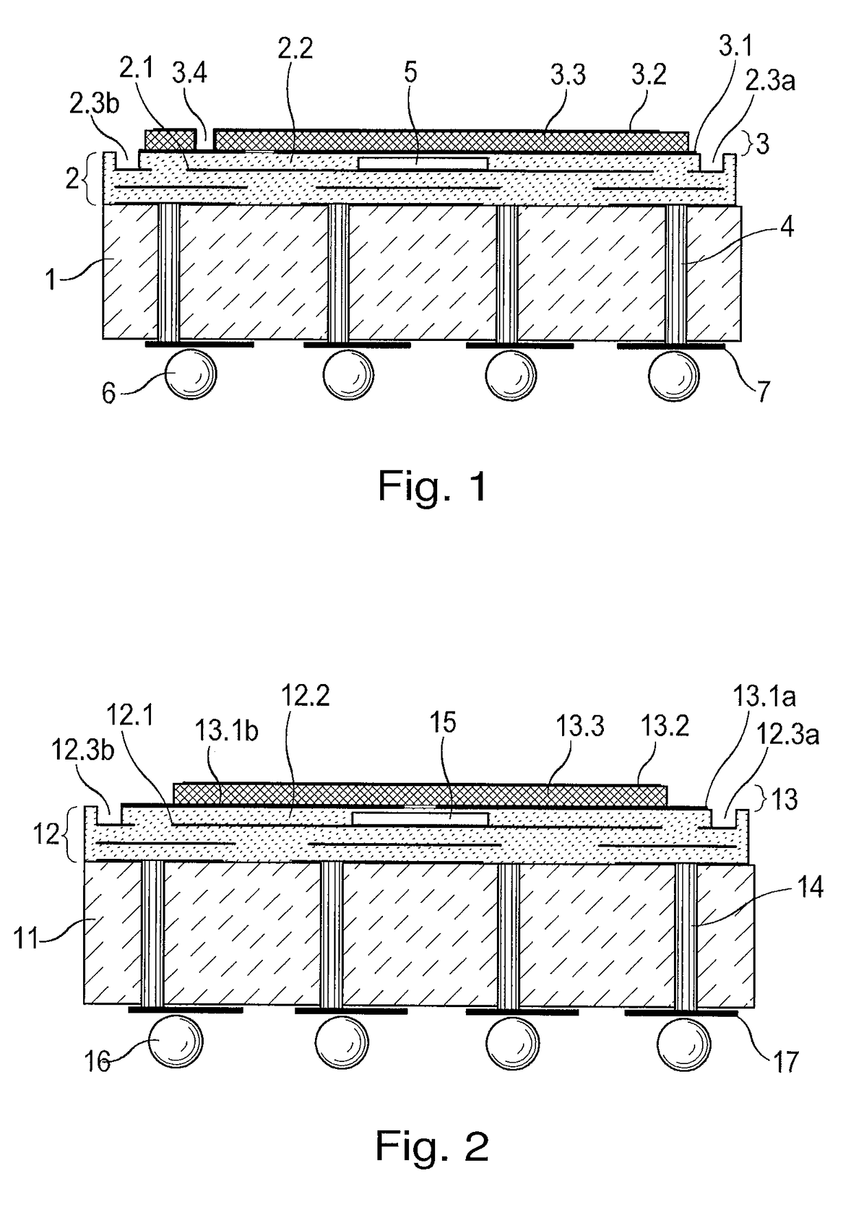
[0036]In FIG. 1, a first exemplary embodiment of a moisture sensor arrangement of the present invention is shown highly schematically.

[0037]The moisture sensor arrangement of the present invention includes a plate-like semiconductor substrate 1, such as a silicon substrate, on which the various elements of the moisture sensor arrangement are placed. In the first exemplary embodiment shown in FIG. 1, an integrated signal processing component 2 is disposed on the top side of the semiconductor substrate 1. The signal processing component 2 is constructed as a housingless CMOS layer stack, with which various electronic components for signal processing and signal preparation are integrated. A capacitive moisture sensor 3 is in turn disposed above the signal processing component 2, that is, vertically adjacent to the signal processing component 2. The moisture sensor 3 is electrically conductively connected to the signal processing component 2. The analog measurement signals generated by ...


PUM

PropertyMeasurementUnit
temperatureaaaaaaaaaa
electricallyaaaaaaaaaa
transmissionaaaaaaaaaa

Abstract

A moisture sensor arrangement including a plate-like semiconductor substrate and an integrated signal processing component disposed on a first side of the semiconductor substrate. The moisture sensor arrangement including a capacitive moisture sensor connected electrically conductively to the integrated signal processing component, wherein the capacitive moisture sensor is disposed on either the first side or a second side of the semiconductor substrate that is opposite the first side of the semiconductor substrate. In addition, the plate-like semiconductor substrate includes 1) plated through-holes, by way of which elements on the first side and the second side of the semiconductor substrate are electrically connectable to one another; and 2) a temperature sensor integrated with the integrated signal processing component.

Description

RELATED APPLICATIONS[0001]Applicants claim, under 35 U.S.C. §119, the benefit of priority of the filing date of Apr. 25, 2012 of a German patent application, copy attached, Serial Number 10 2012 008 118.9, filed on the aforementioned date, the entire contents of which is incorporated herein by reference.BACKGROUND[0002]1. Technical Field[0003]The present invention relates to a moisture sensor arrangement.[0004]2. Background Information[0005]From European patent disclosure EP 1 236 038 B1, a sensor arrangement is known which has a sensor, such as a capacitive moisture sensor, on the upper side of a first semiconductor substrate. The capacitive moisture sensor includes two interdigital electrodes placed side-by-side and one dielectric measurement layer which changes its capacitance as a function of moisture. The measurement signals generated in this way are further processed in the semiconductor chip and prepared suitably for transmission to a subsequent electronic unit. This referenc...

Claims


Application Information

Patent Timeline
Patent Type & Authority Patents(United States)
IPC IPC(8): G01N27/22H01L27/04
CPCG01N27/223H01L27/04G01N27/228G01N27/225G01N27/22
Inventor MAYER, ELMARNIESSNER, GEORGRUNCK, JOACHIM
Owner E E ELEKTRONIK GES
Why Eureka
Try Eureka