Methods for providing variable feature widths in a self-aligned spacer-mask patterning process

a technology of self-aligning spacers and patterning processes, which is applied in the direction of semiconductor devices, instruments, photomechanical treatment, etc., can solve the problems of increasing fabrication complexity and cost, inherently difficult to pattern lines with widths greater than the characteristic width, and limited patterning pitch of a single optical lithography step

Inactive Publication Date: 2018-02-06
GLOBALFOUNDRIES US INC
View PDF18 Cites 8 Cited by
  • Summary
  • Abstract
  • Description
  • Claims
  • Application Information

AI Technical Summary

Benefits of technology

[0008]The following presents a simplified summary of the invention in order to provide a basic understanding of some aspects of the invention. This summary is not an exhaustive overview of the invention. It is not intended to identify key or critical elements of the invention or to delineate the scope of the invention. Its sole purpose is to present some concepts in a simplified form as a prelude to the more detailed description that is discussed later.

Problems solved by technology

Existing optical lithography is capable of high-throughput processing, but the patterning pitch of a single optical lithography step is limited.
A challenge for lithography is to devise tools, materials and processes that can reliably, efficiently and quickly pattern structures with smaller dimensions, reduced pitch or varied pitches.
Due to the regular nature of the spacers and the self-aligned process, it is inherently difficult to pattern lines with widths greater than the characteristic width of the patterning process, referred to as the 1× width.
The patterning of wider lines, such as those needed for high current capacity power rails, typically requires additional masking and patterning steps, giving rise to increased fabrication complexity and cost.
Due to the use of multiple patterning technologies, defects may also increase, such as overlay errors, pitch walking, hard mask profile defects, etc.

Method used


Image

  • Methods for providing variable feature widths in a self-aligned spacer-mask patterning process
  • Methods for providing variable feature widths in a self-aligned spacer-mask patterning process
  • Methods for providing variable feature widths in a self-aligned spacer-mask patterning process

Examples


Embodiment Construction

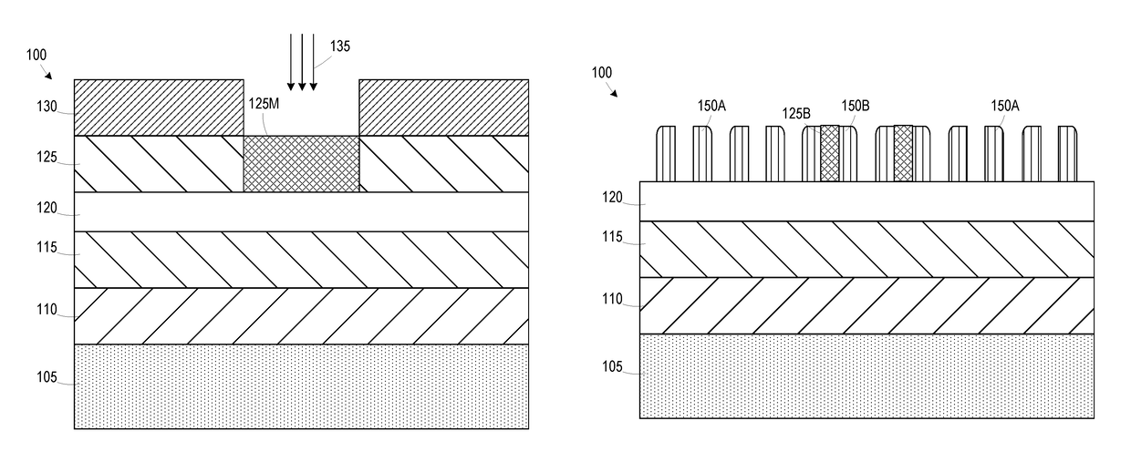
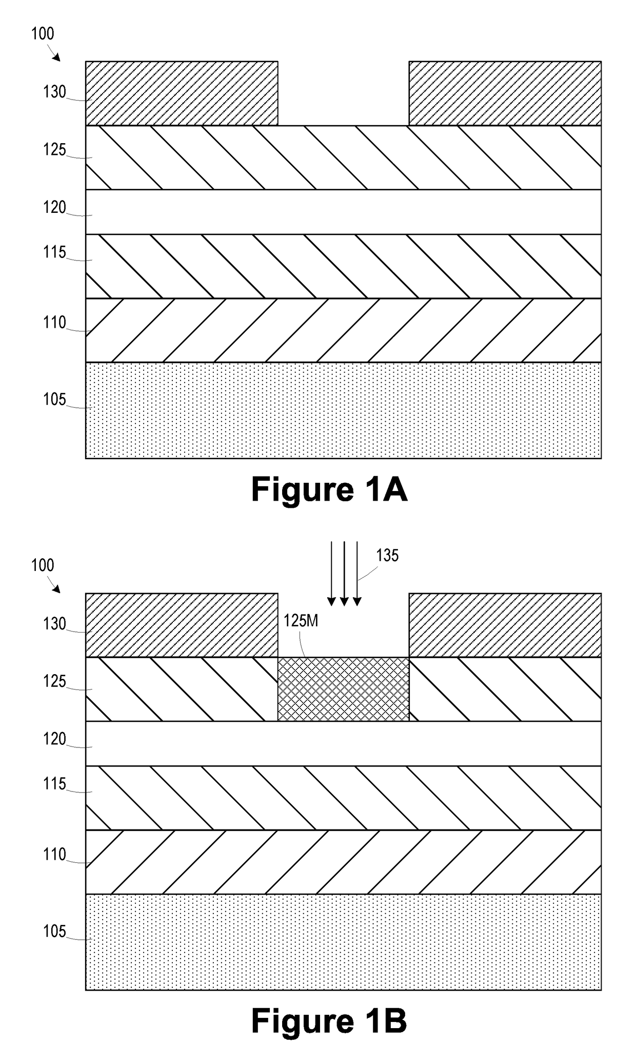
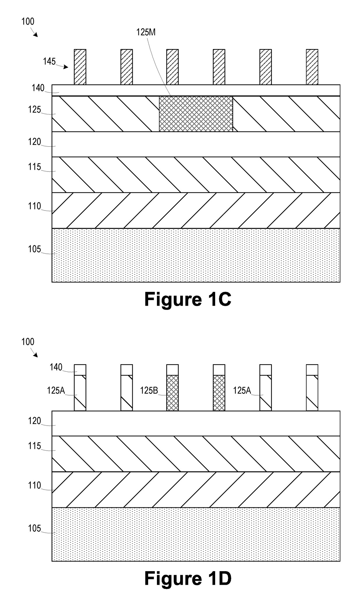
[0017]Various illustrative embodiments of the invention are described below. In the interest of clarity, not all features of an actual implementation are described in this specification. It will of course be appreciated that in the development of any such actual embodiment, numerous implementation-specific decisions must be made to achieve the developers' specific goals, such as compliance with system-related and business-related constraints, which will vary from one implementation to another. Moreover, it will be appreciated that such a development effort might be complex and time-consuming, but would nevertheless be a routine undertaking for those of ordinary skill in the art having the benefit of this disclosure.

[0018]The present subject matter will now be described with reference to the attached figures. Various structures, systems and devices are schematically depicted in the drawings for purposes of explanation only and so as to not obscure the present disclosure with details ...


PUM

PropertyMeasurementUnit
critical dimensionaaaaaaaaaa
widthaaaaaaaaaa
feature widthsaaaaaaaaaa

Abstract

A method includes forming a first mandrel layer above a first process layer. A first implant region is formed in the first mandrel layer. The first mandrel layer is patterned to define a plurality of first mandrel elements. At least a first subset of the first mandrel elements is formed from the first mandrel layer outside the first implant region and a second subset of the first mandrel elements is formed from the first implant region. First spacers are formed on sidewalls of the plurality of first mandrel elements. The first subset of the first mandrel elements are selectively removed without removing the second subset of the first mandrel elements. The first process layer is patterned using the first spacers and the second subset of the first mandrel elements as an etch mask.

Description

BACKGROUND OF THE INVENTION[0001]1. Field of the Invention[0002]The disclosed subject matter relates generally to the fabrication of semiconductor devices and, more particularly, to methods for providing variable feature widths in a self-aligned spacer-mask patterning process.[0003]2. Description of the Related Art[0004]In modern integrated circuits, minimum feature sizes, such as the channel length of field effect transistors as defined by the critical dimension (CD) of the gate electrode, have reached the deep sub-micron range, thereby steadily increasing performance of these circuits in terms of speed and / or power consumption and / or diversity of circuit functions. Existing optical lithography is capable of high-throughput processing, but the patterning pitch of a single optical lithography step is limited. A challenge for lithography is to devise tools, materials and processes that can reliably, efficiently and quickly pattern structures with smaller dimensions, reduced pitch or ...

Claims


Application Information

Patent Timeline
Patent Type & Authority Patents(United States)
IPC IPC(8): H01L21/033H01L21/3115H01L29/66H01L21/3213H01L21/8234G03F7/00H01L21/308
CPCH01L21/823437H01L21/0337H01L21/32139H01L21/0332H01L29/6656H01L29/6653H01L21/31155H01L21/0338G03F7/0002H01L21/3081H01L21/3086H01L21/3088H01L21/823456H01L27/088
Inventor WALLNER, JINZHUANG, HAOREN
Owner GLOBALFOUNDRIES US INC
Why Eureka
Try Eureka