Plasma processing apparatus and operating method of plasma processing apparatus

a plasma processing and plasma technology, applied in semiconductor/solid-state device testing/measurement, instruments, material analysis, etc., can solve the problems of non-linear processing of in-phase components removed by kalman filters in the conventional technique, not highly accurate determined, etc., to achieve high accuracy and accurately detected

Active Publication Date: 2018-04-03
HITACHI HIGH-TECH CORP
View PDF9 Cites 5 Cited by
  • Summary
  • Abstract
  • Description
  • Claims
  • Application Information

AI Technical Summary

Benefits of technology

[0010]An object of the present invention is to provide a plasma processing device and an operation method for the plasma processing device, which can highly accurately detect a residual film thickness and an etching amount.
[0012]According to the present invention, especially in an etching processing device in the plasma processing device, even if a change in a desired light emission intensity is relatively minute with respect to in-phase components included in a light intensity signal obtained from a processing chamber during a plasma-used processing, a change in the intensity can be highly accurately detected by generating a waveform of a signal in which the in-phase components are reduced. Based on data of the signal generated in this manner, an actual etching amount and end point of a processed layer can be further accurately detected.

Problems solved by technology

The above-described conventional technique has a problem since the following points are insufficiently considered.
When such artifacts are generated, an end point indicated as a change in relatively small light emission intensity is buried into a change by the artifacts and is not highly accurately determined.
Further, removal of in-phase components by the Kalman filter in the conventional technique is non-linear processing.
Therefore, since a waveform indicated by time-series data of original light emission intensity is distorted, a change in the intensity corresponding to the above-described end point is buried into this distortion, and the end point cannot be determined at a high accuracy.

Method used


Image

  • Plasma processing apparatus and operating method of plasma processing apparatus
  • Plasma processing apparatus and operating method of plasma processing apparatus
  • Plasma processing apparatus and operating method of plasma processing apparatus

Examples


first example

[0026]An example of the present invention will be described with reference to FIGS. 1 to 4.

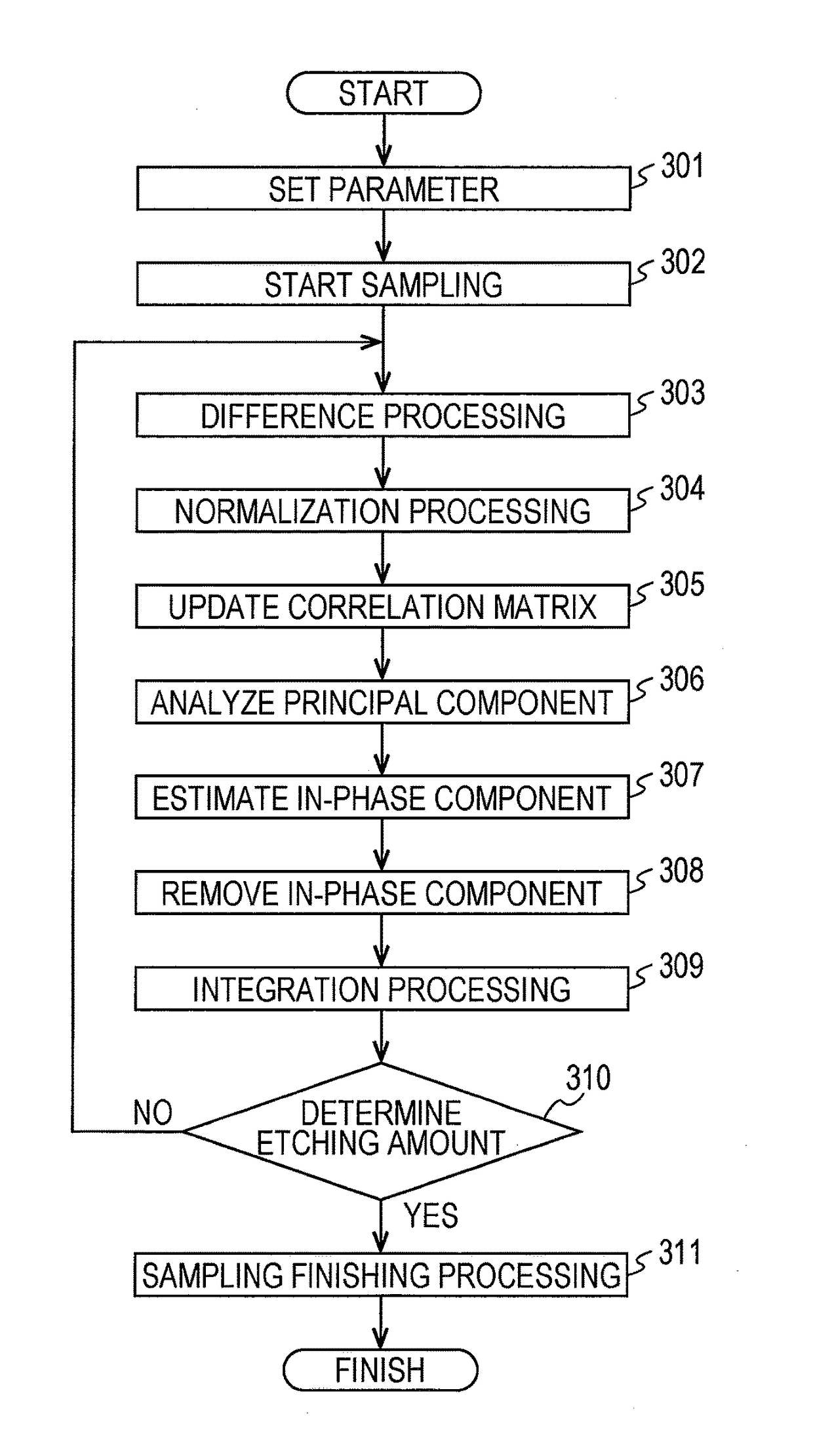
[0027]A configuration of the plasma processing device according to the example will be described with reference to FIG. 1. FIG. 1 is a diagram schematically illustrating an outline of a configuration of a plasma processing device according to the example of the present invention. Especially, a plasma processing device 100 according to the example is a device used in a process to manufacture a semiconductor device by performing an etching processing on a substrate-like sample such as a semiconductor wafer carried in a processing chamber disposed therein. The plasma processing device 100 is a plasma etching device including a detector for detecting an etching amount of the treated sample, for example, a residual film thickness of a mask and a film layer to be processed and the depth of a groove or a hole formed by etching and controlling processing of a sample such as a semiconductor wafer based...


PUM

PropertyMeasurementUnit
wavelengthsaaaaaaaaaa
time-aaaaaaaaaa
light intensityaaaaaaaaaa

Abstract

A plasma processing device performing etching processing to a sample disposed in a processing chamber disposed in a vacuum vessel by using plasma formed in the processing chamber includes a light detector, a component detector, and a determination unit. The light detector detects light intensity of a plurality of wavelengths from the inside of the processing chamber at a plurality of times during the sample processing. The component detector detects, by using a result of a principal component analysis of time-series data, a highly correlated component between the time-series data of a plurality of the wavelengths at a certain time in a plurality of the times obtained from output of the light detector. The determination unit determines an amount or an end point of the etching processing based on a change in light intensity of at least one of a plurality of the wavelengths detected by using the time-series data from which the highly correlated component is removed.

Description

BACKGROUND OF THE INVENTION[0001]The present invention relates to a plasma processing device and an operation method for the plasma processing device. The plasma processing device and the operation method are a plasma processing device and a plasma processing method in which a process to manufacture a semiconductor integrated circuit is used, and a substrate-like sample such as a semiconductor wafer disposed in a processing chamber in a vacuum vessel is processed by using plasma formed in the processing chamber. The plasma processing device and the operation method detect a film thickness or a processing amount of a sample surface by using light emission from the inside of the processing chamber detected during the processing.[0002]A process to manufacture a semiconductor device includes processing to form a circuit pattern of a semiconductor device, so-called dry-etching processing, by etching a film structure including a plurality of film layers including a dielectric material and...

Claims


Application Information

Patent Timeline
Patent Type & Authority Patents(United States)
IPC IPC(8): G01B11/06H01L21/3065H01L21/66G01N21/84H01J37/32
CPCH01J37/32972G01B11/0616G01N21/84H01J37/32935H01L21/3065H01L22/26H01J37/32963H01J2237/334H01J37/32715H01J37/32834H01J37/3299H01L21/67253
Inventor KAWAGUCHI, YOHEIUSUI, TATEHITOTOGAMI, MASAHITOINOUE, SATOMINAKAMOTO, SHIGERU
Owner HITACHI HIGH-TECH CORP
Why Eureka
Try Eureka