High-density EEPROM arrays having parallel-connected common-floating-gate NFET and PFET as memory cell

Inactive Publication Date: 2018-04-17
IBM CORP
View PDF3 Cites 2 Cited by
  • Summary
  • Abstract
  • Description
  • Claims
  • Application Information

AI Technical Summary

Benefits of technology

[0004]In accordance with an embodiment, a semiconductor structure is provided. The semiconductor structure includes a first transistor connected to a first terminal, a second transistor connected in parallel to the first transistor and a second terminal, where the first and second transi

Problems solved by technology

However, existing designs for CMOS EEPROM devices suffer from inefficiencies in the application of hot hole injection.
In particular, the use of silicon dioxide as a gate diel

Method used


Image

  • High-density EEPROM arrays having parallel-connected common-floating-gate NFET and PFET as memory cell
  • High-density EEPROM arrays having parallel-connected common-floating-gate NFET and PFET as memory cell
  • High-density EEPROM arrays having parallel-connected common-floating-gate NFET and PFET as memory cell

Examples


Embodiment Construction

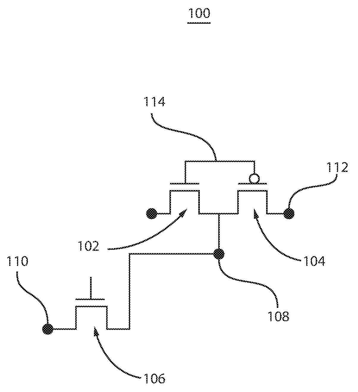
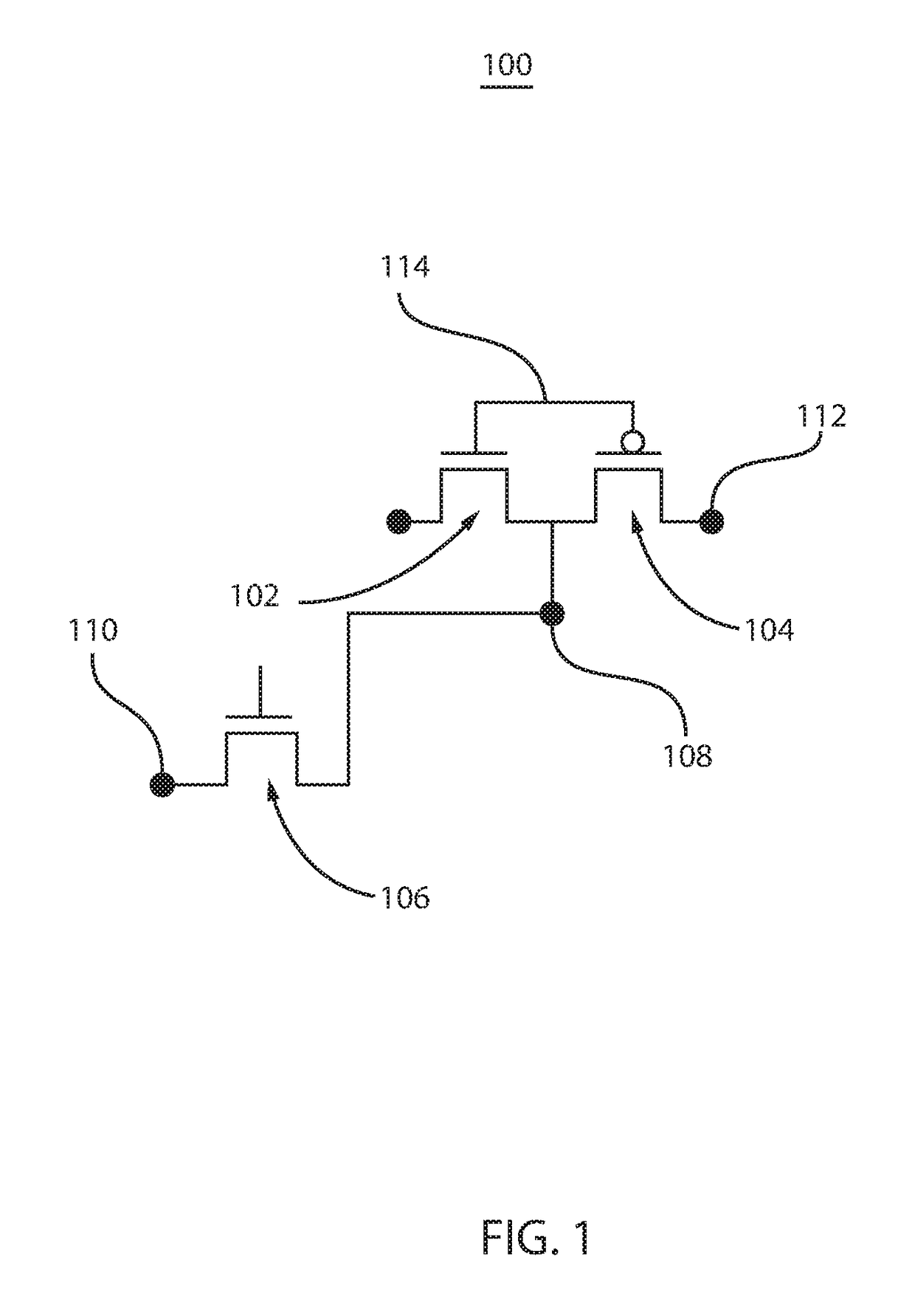
[0017]In one or more embodiments, a semiconductor structure is provided. The semiconductor structure includes a first transistor connected to a first terminal, a second transistor connected in parallel to the first transistor and a second terminal, where the first and second transistors share a common floating gate and a common node, and an access transistor connected in series to the common node and a low voltage terminal, the access transistor configured to trigger hot-carrier injection to the common floating gate to change a voltage of the common floating gate.

[0018]In one or more embodiments, a memory array is provided. The memory array includes an N×M array of memory cells, each memory cell comprising a first transistor connected to a first terminal, a second transistor connected in parallel to the first transistor and a second terminal, where the first and second transistors share a common floating gate and a common node, and an access transistor connected in series to the com...


PUM


Abstract

A memory array includes an N×M array of memory cells, each memory cell having a first transistor connected to a first terminal and a second transistor connected in parallel to the first transistor and a second terminal, where the first and second transistors share a common floating gate and a common output node. Each memory cell further includes an access transistor connected in series to the common output node and a low voltage terminal, the access transistor configured to trigger hot-carrier injection to the common floating gate to change a voltage of the common floating gate. The first transistor is an n-type transistor and the second transistor is a p-type transistor.

Description

BACKGROUNDTechnical Field[0001]The present invention relates generally to programmable CMOS devices, and more specifically, to programmable CMOS devices comprising an NFET and a PFET with a commonly connected floating gate for storing electrical charges and methods of operating the same.Description of the Related Art[0002]Hot carrier injection is a phenomenon in semiconductor devices where a charge carrier (e.g., an electron or a hole) overcomes a potential barrier and, potentially, changes the behavior of a semiconductor device (such as, e.g., a complementary metal oxide semiconductor (CMOS) device). This phenomenon provides one mechanism for the design of an electrically erasable programmable read only memory (EEPROM), where the behavior of the device is stable over time but can be changed by the application of hot carrier injection.[0003]However, existing designs for CMOS EEPROM devices suffer from inefficiencies in the application of hot hole injection. In particular, the use of...

Claims


Application Information

Patent Timeline
IPC IPC(8): G11C16/04G11C16/10H01L27/11521
CPCH01L27/11521G11C16/045G11C16/10G11C16/26H10B41/30
Inventor CHAN, KEVIN K.HEKMATSHOARTABARI, BAHMANNING, TAK H.YAU, JENG-BANG
Owner IBM CORP
Why Eureka
Try Eureka