Substrate with buffer layer for oriented nanowire growth

a nanowire and substrate technology, applied in the direction of nanowire devices, electrical devices, semiconductor devices, etc., can solve the problems of radically altering the thermal profile over the substrate, affecting the performance of the substrate, and unable to readily prevent cracks, so as to avoid costly and time-consuming epitaxy steps in the processing.

Active Publication Date: 2018-04-17
GLO TECH LLC
View PDF28 Cites 1 Cited by
  • Summary
  • Abstract
  • Description
  • Claims
  • Application Information

AI Technical Summary

Benefits of technology

[0027]It is a further advantage of the invention that it makes it possible to grow oriented nanowires on cheaper substrates, such as Si (111) substrates, and in particular Si (100) substrates, but also amorphous substrates, the main prerequisite being the substrate being able to resist the chosen process temperatures.
[0028]Another advantage of the invention is to provide substrates for growing nanowires that can remain in the final device. For example, as mentioned above, in LED structures the substrate is usually removed since it cannot be used in the device, or due to insufficient thermal properties. With for example Si substrates the substrate can remain and be used.
[0029]Yet another advantage with the invention is that costly and time consuming epitaxy steps in the processing are avoided.
[0030]Thanks to the substrate for growing nanowires and the method for growing nanowires of the invention, the next step in development of nitride based semiconductor devices, and in particular GaN-based devices, such as LEDs, will be possible.
[0031]Thus, in one aspect the invention provides a nanowire LED structure, wherein each nanowire in use contributes to the formation of an active region for generation of light.
[0032]Embodiments of the invention are defined in the dependent claims. Other objects, advantages and novel features of the invention will become apparent from the following

Problems solved by technology

However, mismatch between substrate and the nitride semiconductors, for example lattice mismatch, introduce detrimental defects such as cracks in the grown material.
Without this compositionally graded transition layer cracks can not readily be prevented.
However, a buffer layer in accordance with prior art introduces substrate bowing due to the strain, which radically alters the thermal profile over the substrate.
The problem of substrate bowing is enhanced by increasing size of the substrate, in this way being an obstacle for large-scale processing of GaN devices on large substrates.
Growth of the buffer layer is a time consuming procedure and often thick AlN is used in the buffer layer, which limits the vertical conductivity.
Moreover, for many optoelectronic devices, for example LEDs the substrate is often removed, leaving only the buffer layer in the final device, whereby the costly substrate material only is used for the growth step.
Bragg reflectors comprise repeated epitaxial semiconductor layers with different refraction index forming a. Bragg reflectors are limited in their reflectivity over a narrow span of wavelength and incident light angle and are not suitable for devices emitting light in a wider wavelength region.
However, growth of Bragg reflectors is time consuming, and particularly challenging on lattice mismatched substrates, since the crystal quality has to be high to make efficient reflectors.

Method used


Image

  • Substrate with buffer layer for oriented nanowire growth
  • Substrate with buffer layer for oriented nanowire growth
  • Substrate with buffer layer for oriented nanowire growth

Examples


Embodiment Construction

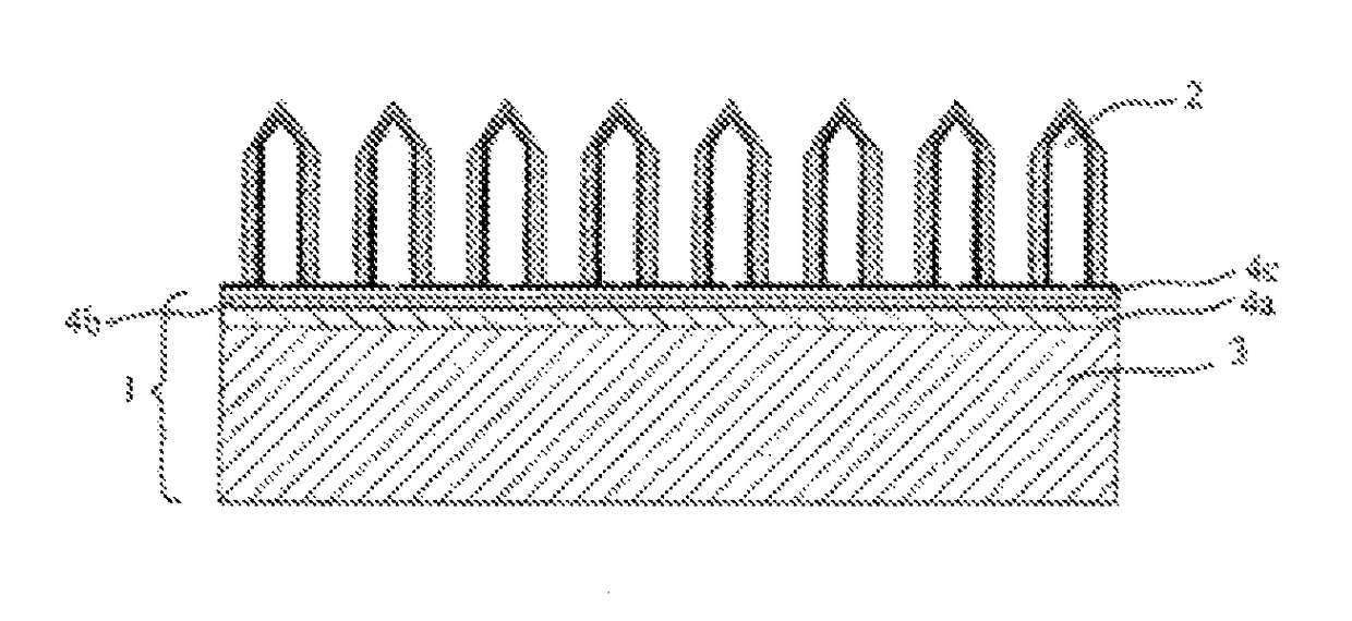
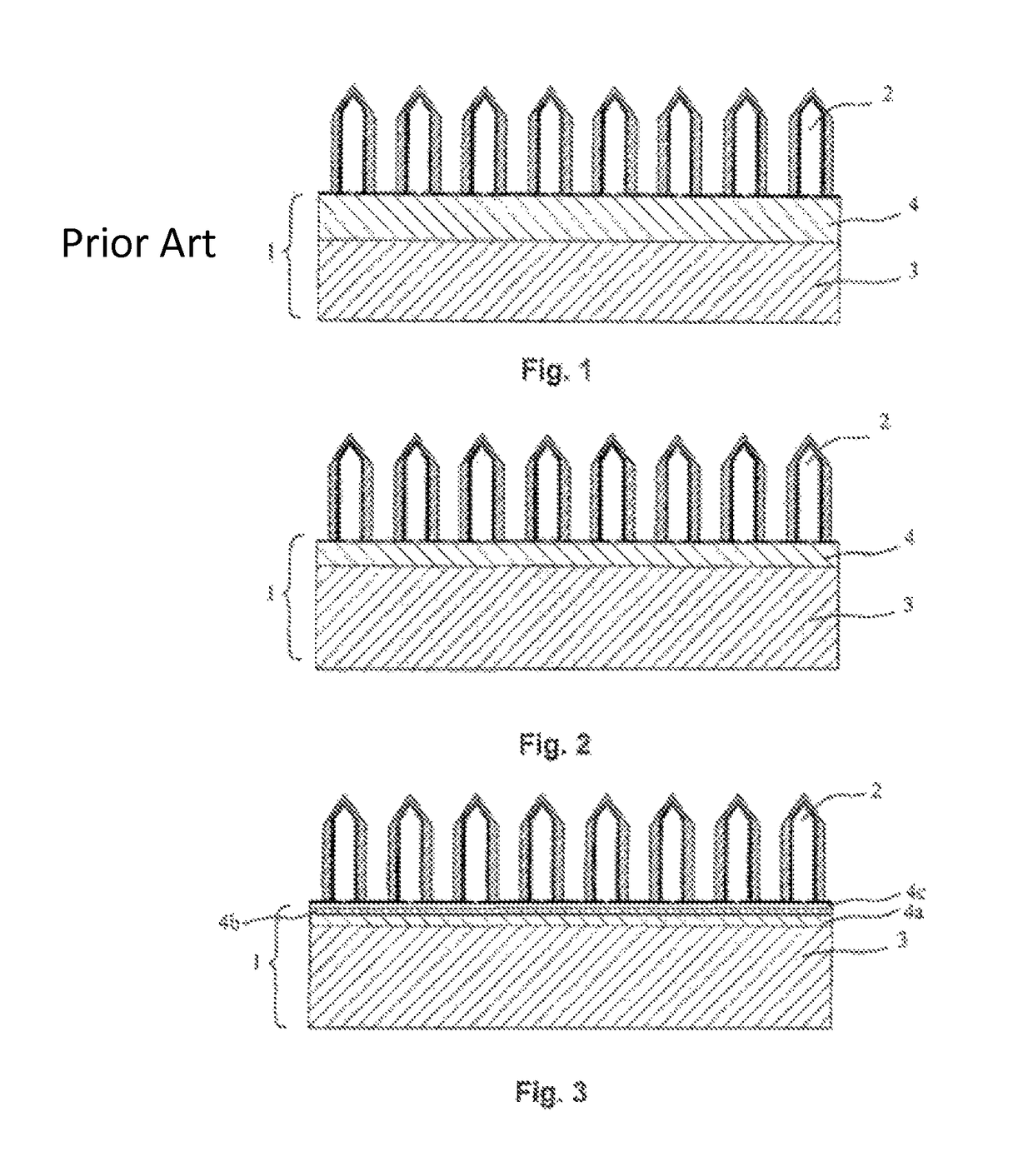
[0040]All references to vertical, lateral etc. are introduced for the ease of understanding only, and should not be considered as limiting to specific orientation. Furthermore, the dimensions of the structures in the drawings are not necessarily to scale.

[0041]Although the preferred embodiment of the invention in the following are described mainly in terms of nanowire light emitting diodes (LEDs) and the needs for such structures it should be appreciated that the substrates and buffer layers of the invention and the nanowire growth thereon can be used to fabricate other optoelectronic devices and electronic devices and to fulfill the needs thereof.

[0042]For LEDs nitride-based semiconductor materials are of great interest at least for the part of the device that generates the light. Typical GaN nanowire LED fabrication includes elevated growth temperatures around 1000 deg C. Substrate / buffer layer materials must be chosen according to this thermal envelope. Examples of such materials...


PUM

PropertyMeasurementUnit
thicknessaaaaaaaaaa
thicknessaaaaaaaaaa
thicknessaaaaaaaaaa

Abstract

The present invention provides a substrate (1) with a bulk layer (3) and a buffer layer (4) having a thickness of less than 2 μm arranged on the bulk layer (3) for growth of a multitude of nanowires (2) oriented in the same direction on a surface (5) of the buffer layer (4). A nanowire structure, a nanowire light emitting diode comprising the substrate (1) and a production method for fabricating the nanowire structure is also provided. The production method utilizes non-epitaxial methods for forming the buffer layer (4).

Description

CROSS-REFERENCE TO RELATED APPLICATIONS[0001]This application is a National Stage application of PCT International Application Serial No. PCT / SE2011 / 050845, filed Jun. 27, 2011, which claims priority from Swedish Application No. 1050700-2, filed Jun. 24, 2010.TECHNICAL FIELD OF THE INVENTION[0002]The present invention relates to nanowire based devices and in particular to substrates for nanowire growth.BACKGROUND OF THE INVENTION[0003]In nanowire based devices, such as nanowire based light emitting diodes (LEDs), a multitude of nanowire based structures are usually arranged in ordered arrays on a substrate. The substrate often has multiple purposes, i.e. being a template for nanowire growth, being a carrier for the nanowires in the device and electrically connecting the nanowires on one side thereof. Different techniques for growth of the ordered arrays of nanowire based structures, where all structures are parallel and oriented in the same direction, are known. For example, semicon...

Claims


Application Information

Patent Timeline
Patent Type & Authority Patents(United States)
IPC IPC(8): H01L33/12H01L21/02B82Y10/00H01L29/06H01L33/18B82Y99/00H01L33/08H01L33/06H01L33/00B82Y40/00B82Y20/00H01L33/24
CPCH01L33/12H01L21/0237H01L21/0254H01L21/02439H01L21/02444H01L21/02458H01L21/02488H01L21/02513H01L21/02603H01L29/0665H01L29/0676H01L29/0684H01L33/18B82Y10/00Y10S977/762B82Y20/00B82Y40/00B82Y99/00H01L33/007H01L33/06H01L33/08H01L33/24
Inventor OHLSSON, JONAS
Owner GLO TECH LLC
Why Eureka
Try Eureka