Power converting device

a power conversion device and power technology, applied in the direction of electric variable regulation, process and machine control, instruments, etc., can solve the problems of increasing device cost, increasing device cost, and large reverse recovery loss, and achieve small reverse recovery loss, low forward voltage drop, and small conduction loss

Active Publication Date: 2018-05-22
FUJI ELECTRIC CO LTD
View PDF12 Cites 1 Cited by
  • Summary
  • Abstract
  • Description
  • Claims
  • Application Information

AI Technical Summary

Benefits of technology

[0024]Meanwhile, a forward voltage drop of a diode is of a fixed magnitude that does not depend on current. Because of this, there is a limit to a reduction of conduction loss even when a number of the diode 4 of FIG. 6 to FIG. 8 connected in parallel is increased. In particular, although a fast recovery diode has an advantage in that reverse recovery loss is small, a forward voltage drop is large in comparison with that of a so-called rectifying diode, which has an object of rectifying a commercial frequency.
[0026]Also, when using a diode formed of a WBG material, such as a Schottky barrier diode, this kind of diode is expensive in comparison with a diode formed of a silicon material, and causes an increase in device cost.
[0029]Therefore, the disclosure provides a power converting device such that semiconductor device conduction loss and reverse recovery loss are reduced to an utmost, and overall efficiency is increased, and, moreover, increase in device size and cost is prevented.
[0037]According to the disclosure, a series circuit of a rectifying diode, which has small conduction loss, and a second semiconductor switching device is connected in parallel with a fast recovery diode, which has small reverse recovery loss, and forward current before reverse recovery occurs is blocked by the second semiconductor switching device. Because of this, reverse recovery of the rectifying diode is avoided, and a low forward voltage drop characteristic of the rectifying diode is utilized, whereby an increase in efficiency of a power converting device can be realized.

Problems solved by technology

Consequently, when combating by replacing a fast recovery diode with a rectifying diode, connecting rectifying diodes in parallel, or the like, the rectifying diode causes an extremely large reverse recovery loss, because of which the object of increasing efficiency cannot be achieved.
Also, when using a diode formed of a WBG material, such as a Schottky barrier diode, this kind of diode is expensive in comparison with a diode formed of a silicon material, and causes an increase in device cost.
Furthermore, the third related art technology shown in FIG. 8 has a problem in that the further the device capacity increases, the further the sizes of the current limiting resistor 51 and short-circuiting switch 52 increase.
In order to prevent these accidents, a countermeasure such as connecting another switch in series with the resistor 51 or providing a temperature fuse is necessary, and there is a problem in that this leads to a further increase in device size and cost.

Method used


Image

  • Power converting device
  • Power converting device
  • Power converting device

Examples


first embodiment

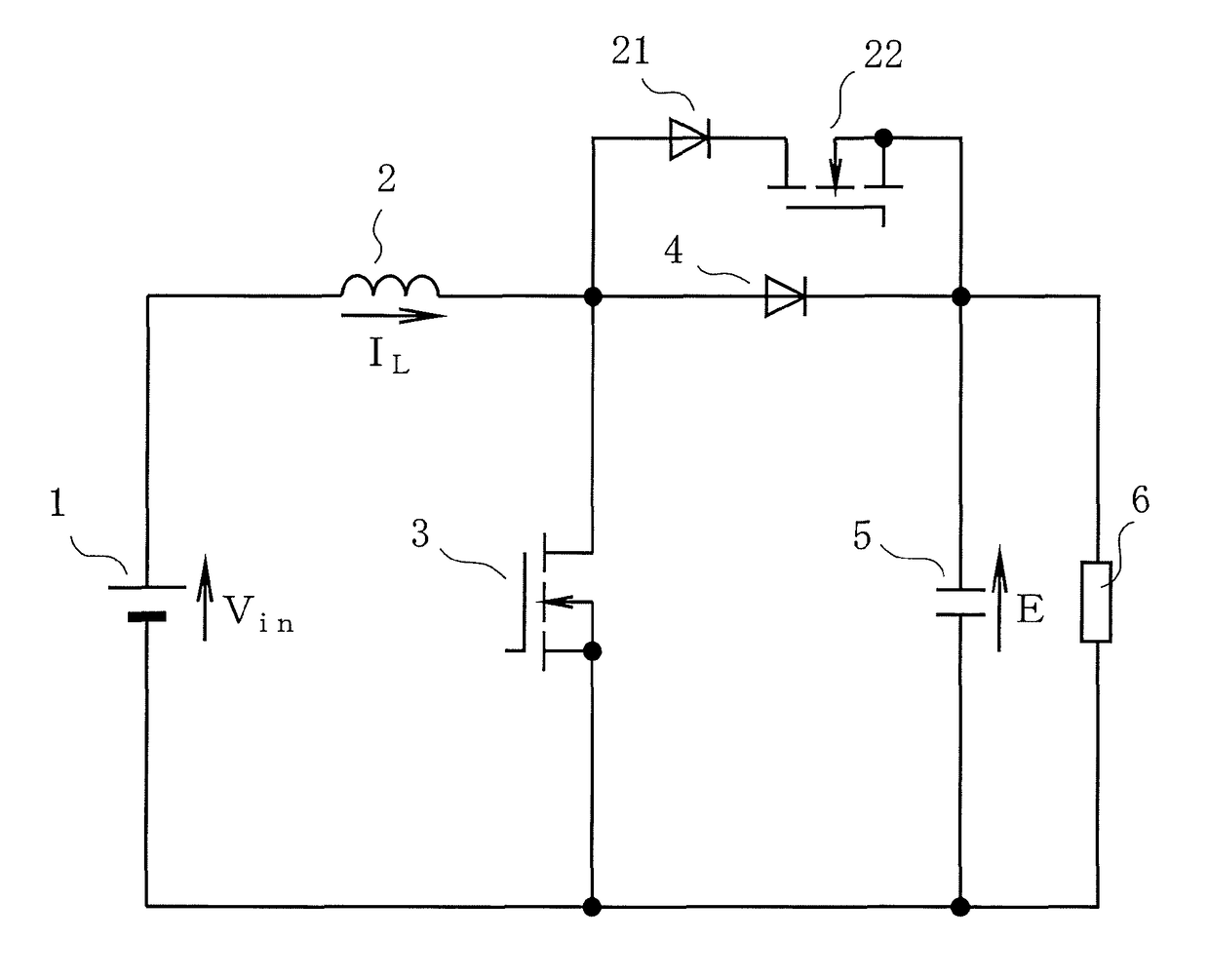
[0047]FIG. 1 is a circuit diagram showing the disclosure. Although one portion of the circuit of FIG. 1 is the same as FIG. 6, an overall configuration of the circuit of FIG. 1 will be described hereafter in order to clarify the embodiment.

[0048]In FIG. 1, a inductor 2, diode 4, and capacitor 5 are connected in series to both ends of a direct current power supply 1, and a load 6 is connected in parallel with the capacitor 5. Also, a first semiconductor switching device 3 is connected between an anode of the diode 4 and a negative electrode of the direct current power supply 1. Furthermore, a series circuit of a rectifying diode 21 and second semiconductor switching device 22 is connected in parallel with the diode 4.

[0049]Herein, MOSFETs are used as the semiconductor switching devices (hereafter referred to simply as switching devices) 3 and 22. Also, the diode 4 is, for example, a fast recovery diode.

[0050]A basic operation of this circuit is the same as that of the previously desc...

second embodiment

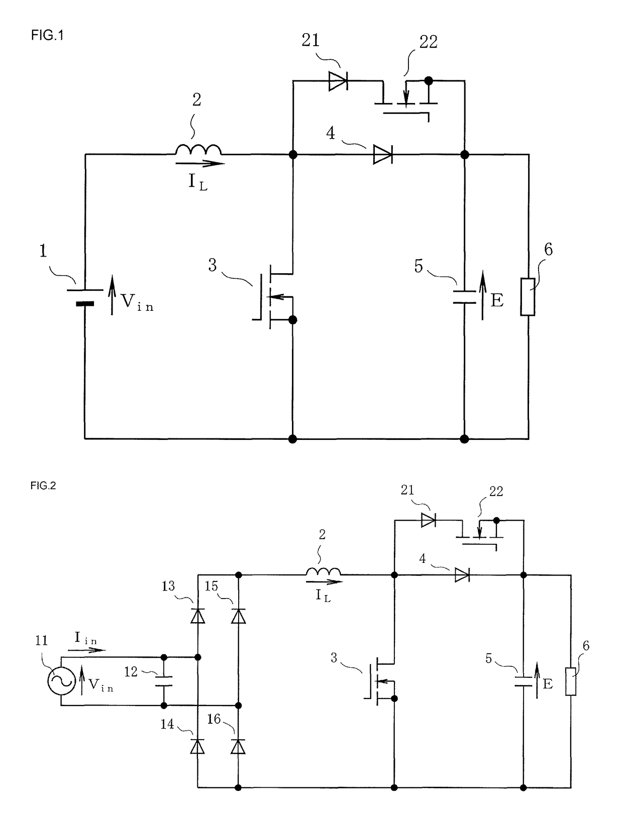
[0061]Next, FIG. 2 is a circuit diagram showing the disclosure.

[0062]The second embodiment is an example wherein a rectifying power supply is used in place of the direct current power supply 1 of FIG. 1, and the rectifying power supply is configured of a bridge rectifier circuit formed of an alternating current power supply 11 and rectifying diodes 13 to 16, in the same way as in FIG. 7. 12 is a filtering capacitor.

[0063]This circuit is well-known as a PFC (power factor correction) circuit, and by utilizing the characteristic of the current IL being arbitrarily controllable, as previously described, the voltage E can be kept at a desired value while arranging that the input current Iin is a sine wave in phase with the input voltage Vin.

[0064]As operations of the diodes 4 and 21 and switching device 22 are the same as in the first embodiment, a description thereof will be omitted.

[0065]The circuit of FIG. 2 is such that when recovering from a momentary voltage drop of the alternating...

third embodiment

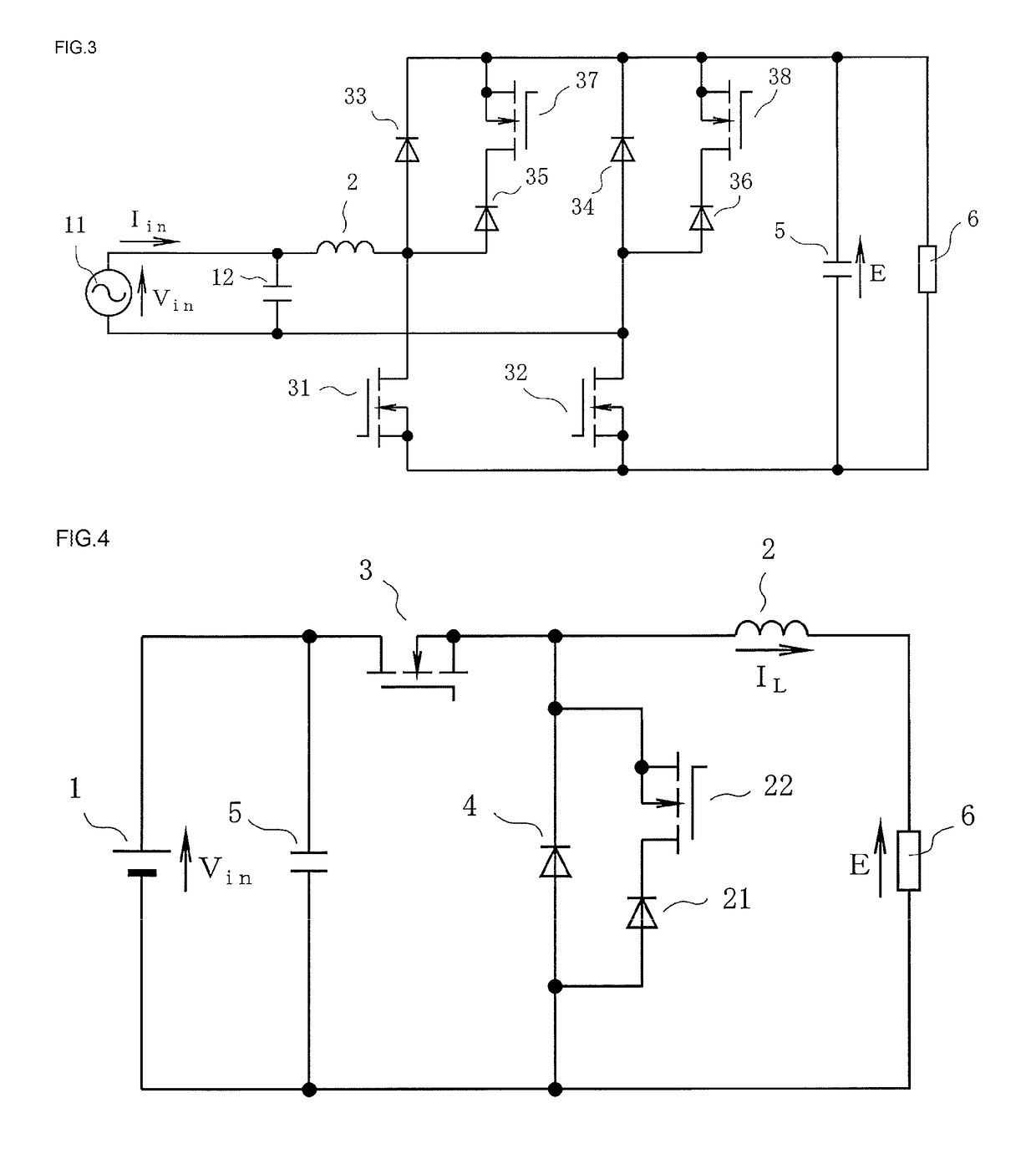
[0070]Next, FIG. 3 is a circuit diagram showing the disclosure. This embodiment is an example wherein the disclosure is applied to a so-called bridgeless PFC circuit that does not need a bridge rectifier circuit.

[0071]In FIG. 3, the capacitor 12 is connected to both ends of the direct current power supply 11, and one end of the capacitor 12 is connected via the inductor 2 to a series connection point of a diode (fast recovery diode) 33 and switching device 31. A series circuit of a diode (fast recovery diode) 34 and switching device 32, the capacitor 5, and the load 6 are connected in parallel to the series circuit of the diode 33 and switching device 31.

[0072]Herein, the switching devices 31 and 32 correspond to a first semiconductor switching device in the claims.

[0073]Also, a series circuit of a switching device 37 and rectifying diode 35 is connected in parallel with the diode 33, and a series circuit of a switching device 38 and rectifying diode 36 is connected in parallel with...


PUM


Abstract

A power converting device, in one possible configuration, includes a chopper circuit with a first semiconductor switching device, a fast recovery diode, and an inductor of which one end is connected to a connection point connecting between the first semiconductor switching device and fast recovery diode; a series circuit, connected in parallel with the fast recovery diode, including a rectifying diode with a greater reverse recovery loss and a smaller forward voltage drop than those of the fast recovery diode, and a second semiconductor switching device. The second semiconductor switching device has a lower breakdown voltage and a smaller forward voltage drop than those of the first semiconductor switching device, is configured to turn on when the first semiconductor switching device is turned off, and is configured to turn off at a timing before the first semiconductor switching device shifts from an off-state to an on-state.

Description

CROSS-REFERENCE TO RELATED APPLICATIONS[0001]This application is a continuation application, filed under 35 U.S.C. § 111(a), of International Application PCT / JP2016 / 062196 filed on Apr. 18, 2016 and claims foreign priority to Japanese Patent Application No. 2015-117890, filed Jun. 11, 2015, the content of each of which is incorporated herein by reference in its entirety.BACKGROUND1. Field[0002]The present disclosure relates to technology for reducing loss in a semiconductor device, thereby achieving increased efficiency of a power converting device.2. Related Art[0003]FIG. 6 is a circuit diagram showing a first related art technology of a power converting device, which is well-known as a step-up chopper circuit. In FIG. 6, 1 is a direct current power supply, 2 is a inductor, 3 is a semiconductor switching device (hereafter referred to simply as a switching device) formed of a MOSFET, 4 is a diode, 5 is a capacitor, and 6 is a load.[0004]Herein, an IGBT (insulated gate bipolar transi...

Claims


Application Information

Patent Timeline
Patent Type & Authority Patents(United States)
IPC IPC(8): H02M3/135H02M3/155H02M7/12H02M1/08H02M7/162H02M1/00
CPCH02M3/155H02M1/08H02M7/12H02M7/162H02M3/135H02M2001/0054Y02B70/10H02M1/32H02M1/4225H02M1/0085H02M1/0054
Inventor YAMADA, RYUJI
Owner FUJI ELECTRIC CO LTD
Why Eureka
Try Eureka