Process for creating high efficiency photovoltaic cells

a photovoltaic cell, high-efficiency technology, applied in the direction of basic electric elements, electrical apparatus, semiconductor devices, etc., can solve the problems of reducing the conversion efficiency, the toxic nature of si-solar cells is of great concern for the environment, and the si-solar cell is not yet widely accepted as an alternative source of energy

Active Publication Date: 2018-06-05
BANPIL PHOTONICS
View PDF51 Cites 1 Cited by
  • Summary
  • Abstract
  • Description
  • Claims
  • Application Information

AI Technical Summary

Benefits of technology

[0020]According to this invention, it is an object to provide the solar cell structure to reduce the carriers-recombination and also to increase the absorption of the light by increasing the effective junction area, which increases the photo-generated carriers.
[0028]It is also another object of this invention to provide a low-cost manufacturing process for the photovoltaic cell.

Problems solved by technology

Although the fabrication processes of amorphous silicon based photovoltaic cells is rather simple and inexpensive, one notable downside of this type of cell is its vulnerability to defect-induced degradation that decreases its conversion efficiency.
However, due to the high cost ($3 to $5 / Watt) of today's Si-based solar cell, the Si-solar cell is not yet widely accepted as an alternative source of energy.
However, the toxic nature of these materials is of great concern for the environment.
This again raises issues associated with the toxicity of these materials and their threat to the environment.
The synthesis processes of single crystalline group III-V is, in general, very costly because of substantial complications involved in epitaxial growth of group III-V single crystalline compound semiconductors.
All types of photovoltaic cells described above, no matter what materials the cell is made of, essentially fall into one specific type of structure that usually limits its power generation capability.
However, if the p-type layer 101 is too thick, electrons 106e generated at the region far away from the pn-junction 103 cannot be collected efficiently due to many adverse recombination processes that prevent photo generated carriers from diffusing into the pn-junction 103, significantly decreasing PCCE.
Thus, the basic structure of current photovoltaic cells severely limits increasing the conversion efficiency.
However, this makes the solar cell heavier and more costly.
This requires an additional component with the solar cell to concentrate the solar spectrum and increases the cost.
In addition, today's solar cell materials are not highly radiation-tolerant.

Method used


Image

  • Process for creating high efficiency photovoltaic cells
  • Process for creating high efficiency photovoltaic cells
  • Process for creating high efficiency photovoltaic cells

Examples


Embodiment Construction

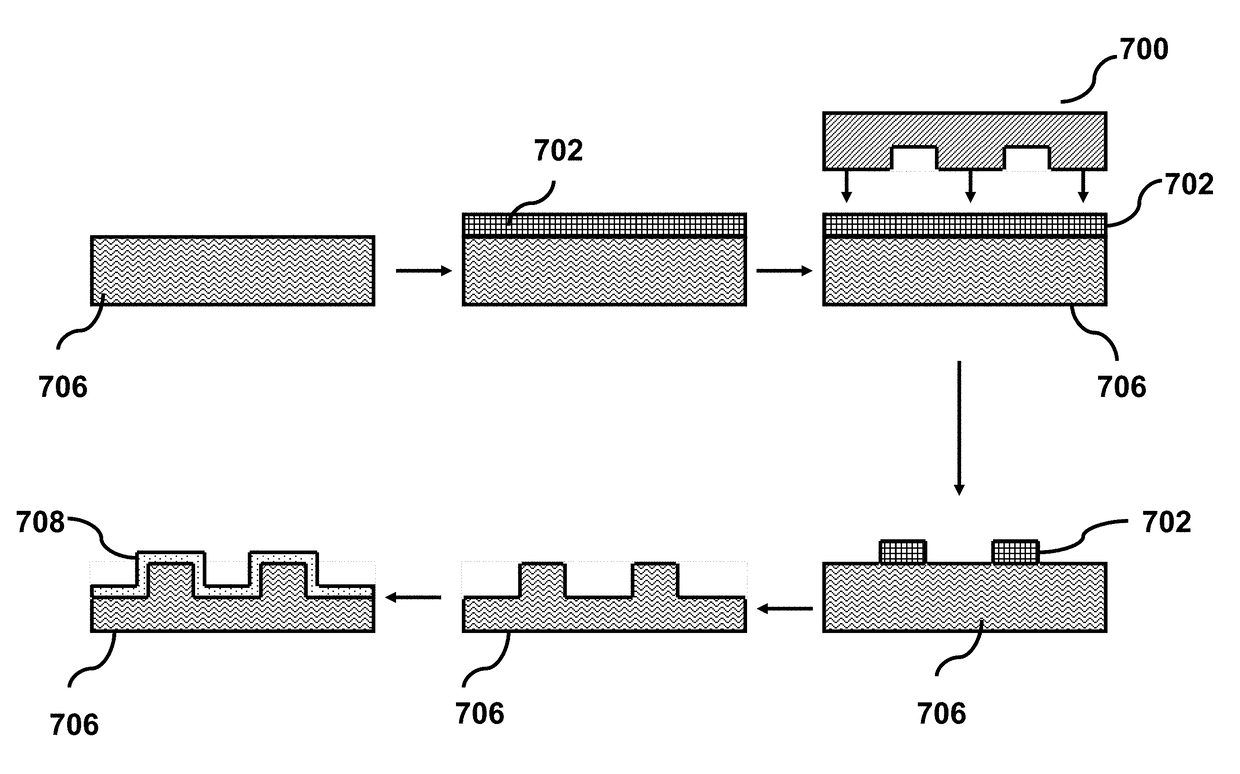
[0039]The following described process is a manufacturing sequence that results in a solar cell with a patterned structure designed to self intensify the light that is incident on the surface of the cell. These shapes are myriad and depend on the incident light to be captured and how it alters its angle with respect to the surface. Some examples of suitable shapes are a trapezoidal pyramid, a pyramid, and a cylinder. These shapes are given as examples and are not to be considered limiting of the type of structures that can be made. There are several processes that produce several structures with the same intensifying effects. These processes are described in detail in the following paragraphs.

[0040]Each process requires the construction of a mold that imprints the pattern on the final surface. According to our invention, the mold is made from one of two processes. One method involves creating a plug or buck that is shaped like the desired pattern, and then the final mold is created f...


PUM


Abstract

A novel method to fabricate the high-efficiency solar cells are provided by this application. The cells are based on micro (or nano) structures that not only increase the surface area but also have the capability of self-concentrating the solar spectrum incident onto the cell. These photovoltaic cells have a larger power generation capability per unit physical area than conventional cells. These cells will have enormous applications in space, commercial, residential and industrial sectors.

Description

STATEMENT REGARDING FEDERALLY SPONSORED RESEARCH OR DEVELOPMENT[0001]This invention was made with Government support under contract no. W31P4Q-08-C-0057 awarded by US Army Aviation and Missile Command. The Government has certain rights in the invention.CROSS-REFERENCE TO RELATED APPLICATIONS[0002]Not ApplicableDESCRIPTIONField of Inventions[0003]This patent specification relates to the creation of structures of photovoltaic cells (hereafter also called “solar cells”). More specifically, it relates to creation of solar cells comprising structures for increasing the junction area and creating a self-amplifying and concentrating effect. This process is used to make solar cells for use in commercial, residential, space, and industrial applications for power generation.Background of the Inventions[0004]Photovoltaic cells, where light is converted into electric power, prevail in a wide range of application fields such as consumer electronics, industrial electronics, and space exploration....

Claims


Application Information

Patent Timeline
Patent Type & Authority Patents(United States)
IPC IPC(8): H01L31/072H01L31/0236H01L31/0352
CPCH01L31/0352H01L31/0236H01L31/072H01L31/03529H01L31/0392Y02E10/50
Inventor DUTTA, ACHYUT KUMAR
Owner BANPIL PHOTONICS
Why Eureka
Try Eureka