Sense circuit for reading data stored in nonvolatile memory cells

Inactive Publication Date: 2000-02-22
STMICROELECTRONICS SRL
View PDF23 Cites 39 Cited by
  • Summary
  • Abstract
  • Description
  • Claims
  • Application Information

AI Technical Summary

Benefits of technology

Basically, the device for generating an unbalance between a reference cell branch of the sense circuit and another branch of the circuit comprising the selectively addressed array cell to be read, which is employed is basically a current generator and therefore, as in the case of a currentoffset sense circuit of the prior art, the sizes of the load transistors of the array side and of the reference side of the differential sense circuit

Problems solved by technology

The reduction of the size of the devices poses serious problems to the achievement of these aims.
Clearly the .Iadd.current-unbalance .Iaddend.system .Iadd.of FIG. 2 .Iaddend.has limitations, in static terms, toward the value of VCC.sub.max and this constitutes a drawback.
In fact, while for the case of a load-unbalance system, the current in the two branches (reference side and array side) of the sense circuit are intrinsically different for any value of the gate voltage of the cells (and therefore the circuit provides a correct sensing during a transient), in the case of a current-offset sense circuit, because the circuit is powered at VCC, there is not a transient phase for the value of the current set by the of

Method used


Image

  • Sense circuit for reading data stored in nonvolatile memory cells
  • Sense circuit for reading data stored in nonvolatile memory cells
  • Sense circuit for reading data stored in nonvolatile memory cells

Examples


Embodiment Construction

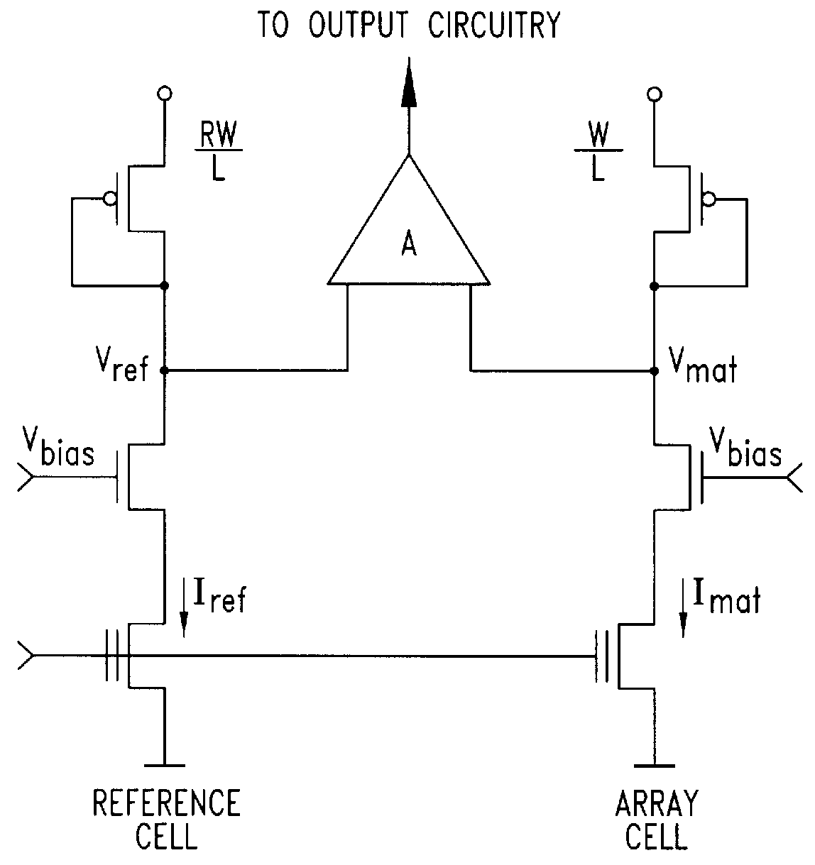
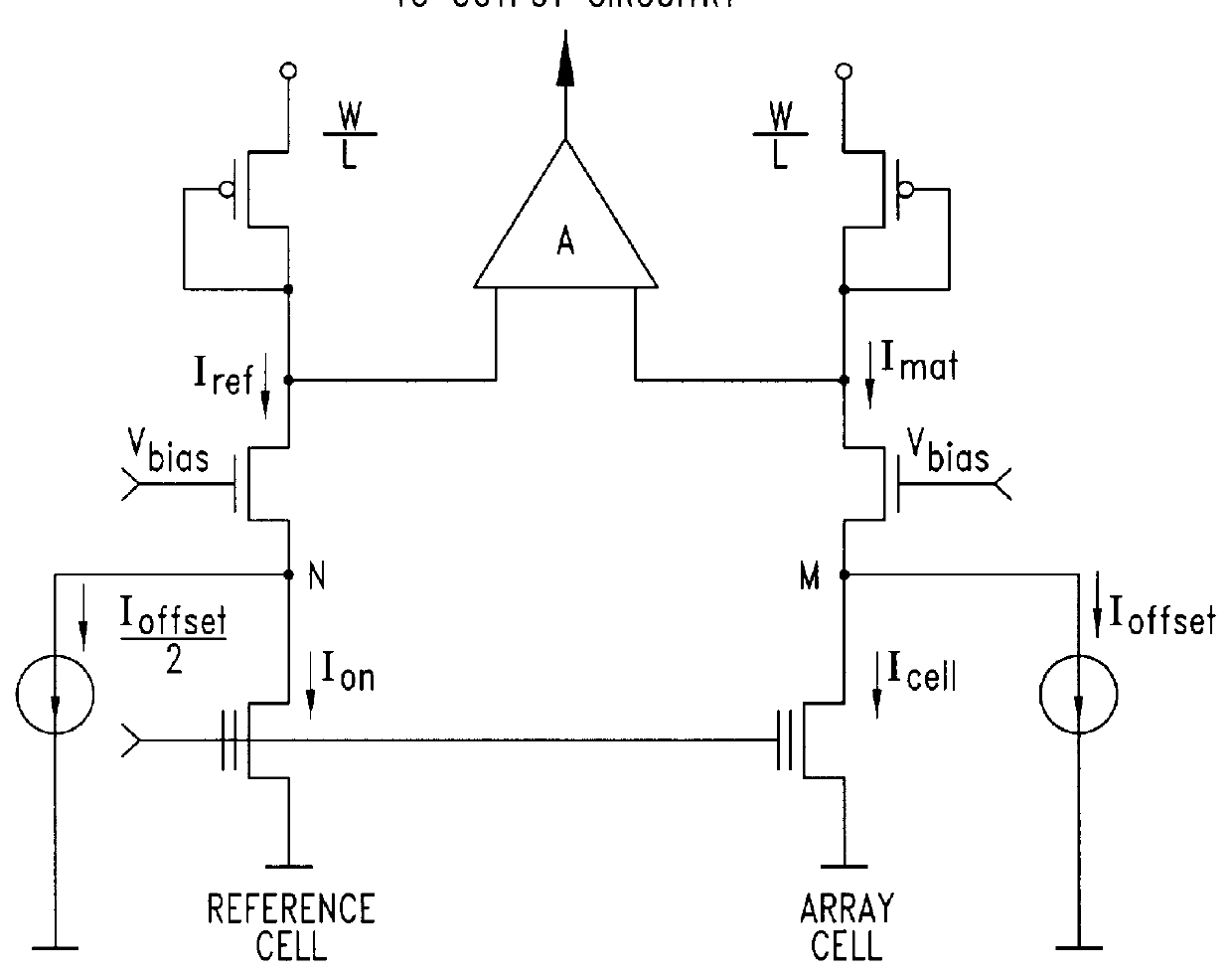
For simplicity's sake, in the circuit diagram of FIGS. 5 and 8, only the offsetting current generating circuit of the offset-current-type sense circuit as shown in FIG. 3 is depicted; the circuit nodes M and N of the circuit of FIG. 3 being indicated in the so-partialized circuit diagrams of FIGS. 5 and 8.

Moreover the label DUMMY ROW used in FIGS. 5 and 8, indicates a drive voltage line derived from a supplementary row of cells of the array of cells which is decoded at every reading and which therefore replicates perfectly the behaviour of .[.anyone.]. .Iadd.current unbalance .Iaddend.row of memory cells of the array which is selected for reading, during a transient.

Normally, the reference column line, REFERENCE BITLINE, serves a certain number of column lines, MATRIX BITLINE, of the array and to these is adjacently formed on the silicon chip so as to make as similar as possible the voltages present on the gate of the reference cell and on the gate of a selected cell of the array al...


PUM


Abstract

A sense circuit for reading EPROM and ROM type memory cells employs a circuit for generating an offsetting current which is exempt of error during transients and which thus permits to achieve a reduced access time. On the other hand, the sense circuit maintains the intrinsic advantages of a current-offset sensing architecture which is represented by a substantially unlimited operating voltage range toward the maximum value VCCmax. The current generating circuit is driven by means of a supplementary row of cells which is decoded at every reading and which replicates, during transients, the behaviour of the row selected for the reading.

Description

BACKGROUND OF THE INVENTIONThe present invention relates to a circuit for reading the information stored in ROM and EPROM type memories according to a differential sensing mode and, in particular to an improved circuit for generating an offsetting current for discriminating between the currents which flow through a certain cell of the memory array which has been selectively addressed for reading and a virgin reference cell, according to a current offset sensing mode.Among semiconductor nonvolatile memories, EPROM memories represent one of the most advanced field of integration in silicon. Starting from nowadays common 1 megabit devices, new devices with a capacity of up to 4 megabit have been presented lately and new ambitious goals are announced.Together with an ever increasing packing density, the memory market requires improved performances in terms of access time, write time and power consumption. The reduction of the size of the devices poses serious problems to the achievement...

Claims


Application Information

Patent Timeline
IPC IPC(8): G11C16/06G11C16/28G11C11/419G11C17/00G11C17/18
CPCG11C16/28
Inventor PASCUCCI, LUIGIOLIVO, MARCO
Owner STMICROELECTRONICS SRL
Why Eureka
Try Eureka