
FPGA integrated circuit having embedded sram memory blocks with registered address and data input sections

a technology of integrated circuits and memory blocks, applied in the field of integrated circuits, can solve the problems of limiting the ability of a given fpga architecture to implement certain speed-critical designs, unable to complete its mission successfully on a first try, and modern fpga's tend to be fairly complex, so as to maximize the data output (data reading) bandwidth of embedded memory, increase the overall system bandwidth, and maximize bandwidth

Inactive Publication Date: 2007-03-13
LATTICE SEMICON CORP
View PDF6 Cites 6 Cited by
  • Summary
  • Abstract
  • Description
  • Claims
  • Application Information

AI Technical Summary

Benefits of technology

The invention is an improved FPGA device that includes multi-ported SRAM blocks for holding run-time storage data. These SRAM blocks have at least one port that can receive address signals and respond by directing the writing or reading of data from that area. The address signals that drive the ports come from sources that have changing output states. The invention provides address-capturing registers for capturing the address signals and data-validating strobe signals for each port, which can enable a changing of the output state of the signal source once the address signal has been captured. This allows for simultaneous read operations at different ports and maximizes the data output bandwidth. The SRAM blocks can begin responding to new address signals even while the destination logic blocks of old data are still busy responding to old data, which further increases overall system bandwidth.

Problems solved by technology

Another part of the interconnect network may be hard wired or nonconfigurable such that it does not allow for programmed definition of the path to be taken by respective signals traveling along such hard wired interconnect.
Read / write speed, data validating speed, and appropriate interconnecting of such on-chip embedded memory to other resources of the FPGA can limit the ability of a given FPGA architecture to implement certain speed-critical designs.
Modern FPGA's tend to be fairly complex.
In various instances, however, the FPGA configuring software may find that it cannot complete its mission successfully on a first try.
This might occur because signal routing resources have been exhausted in one or more congested parts of the designated FPGA device.
For example, signal propagation time may be too large in a speed-critical part of the FPGA-implemented circuit.
More specifically, certain synchronization signals may need to propagate from one section of the FPGA to another according to a particular sequence and architectural constraints of the FPGA device may impede this from happening in an efficient manner in so far as resource utilization is concerned.
Even when relatively powerful, high-speed computers are used, it may take the FPGA configuring software a significant amount of time to find a workable solution.
In some instances, even after having spent a large amount of time trying to find a solution for a given FPGA-implementation problem, the FPGA configuring software may fail to come up with a workable solution and the time spent becomes lost turn-around time.
It may be that, because of packing inefficiencies, the user has chosen too small an FPGA device for implementing too large of an original circuit.
Another possibility is that the internal architecture of the designated FPGA device does not mesh well with the organization and / or timing requirements of the original circuit design.
If after a number of tries, the FPGA configuring software fails to find a workable solution, the user may choose to try again with a differently-structured FPGA device.
Each of these options invariably consumes extra time and can incur more costs than originally planned for.

Method used


Image

  • FPGA integrated circuit having embedded sram memory blocks with registered address and data input sections
  • FPGA integrated circuit having embedded sram memory blocks with registered address and data input sections
  • FPGA integrated circuit having embedded sram memory blocks with registered address and data input sections

Examples


Embodiment Construction

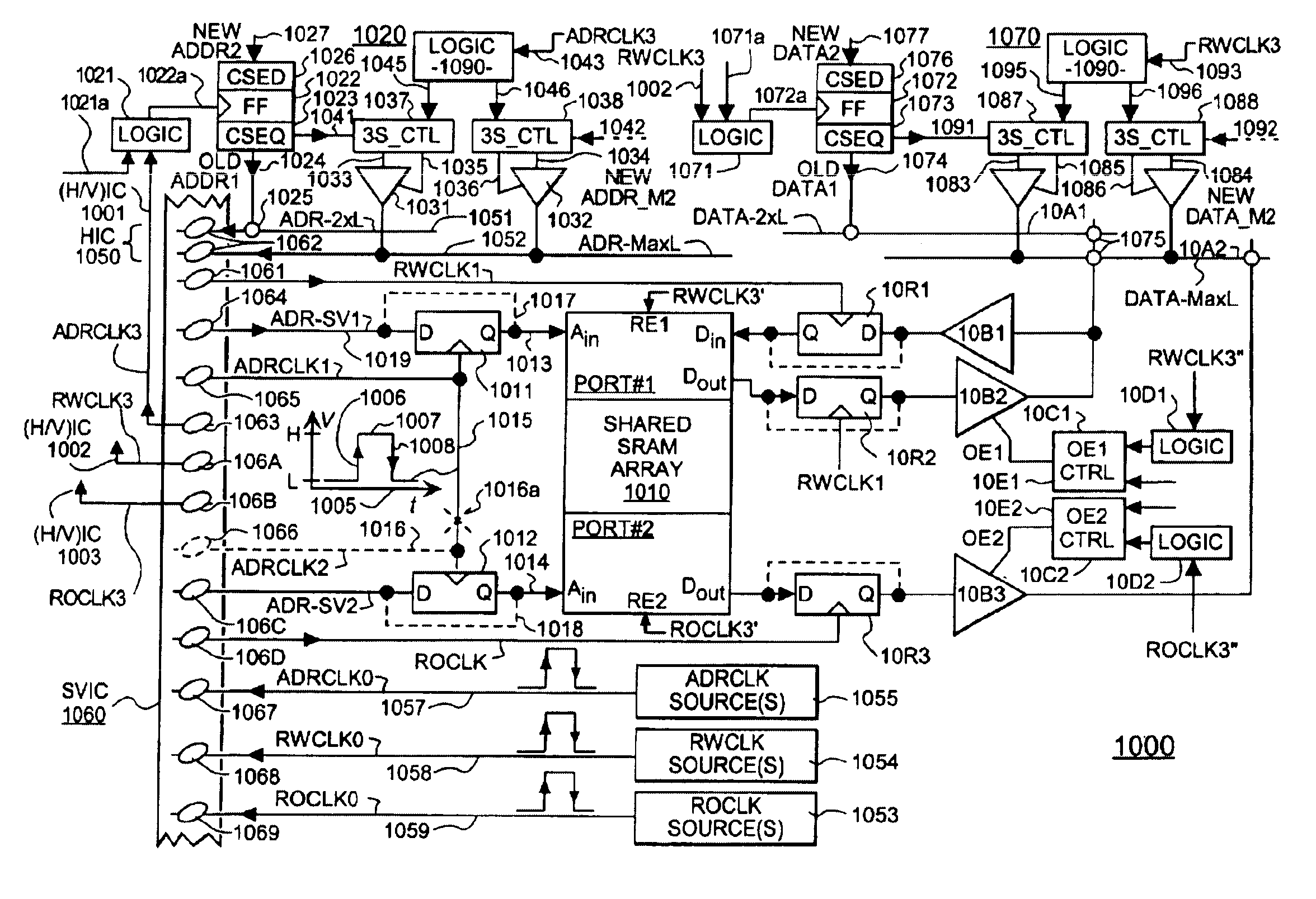
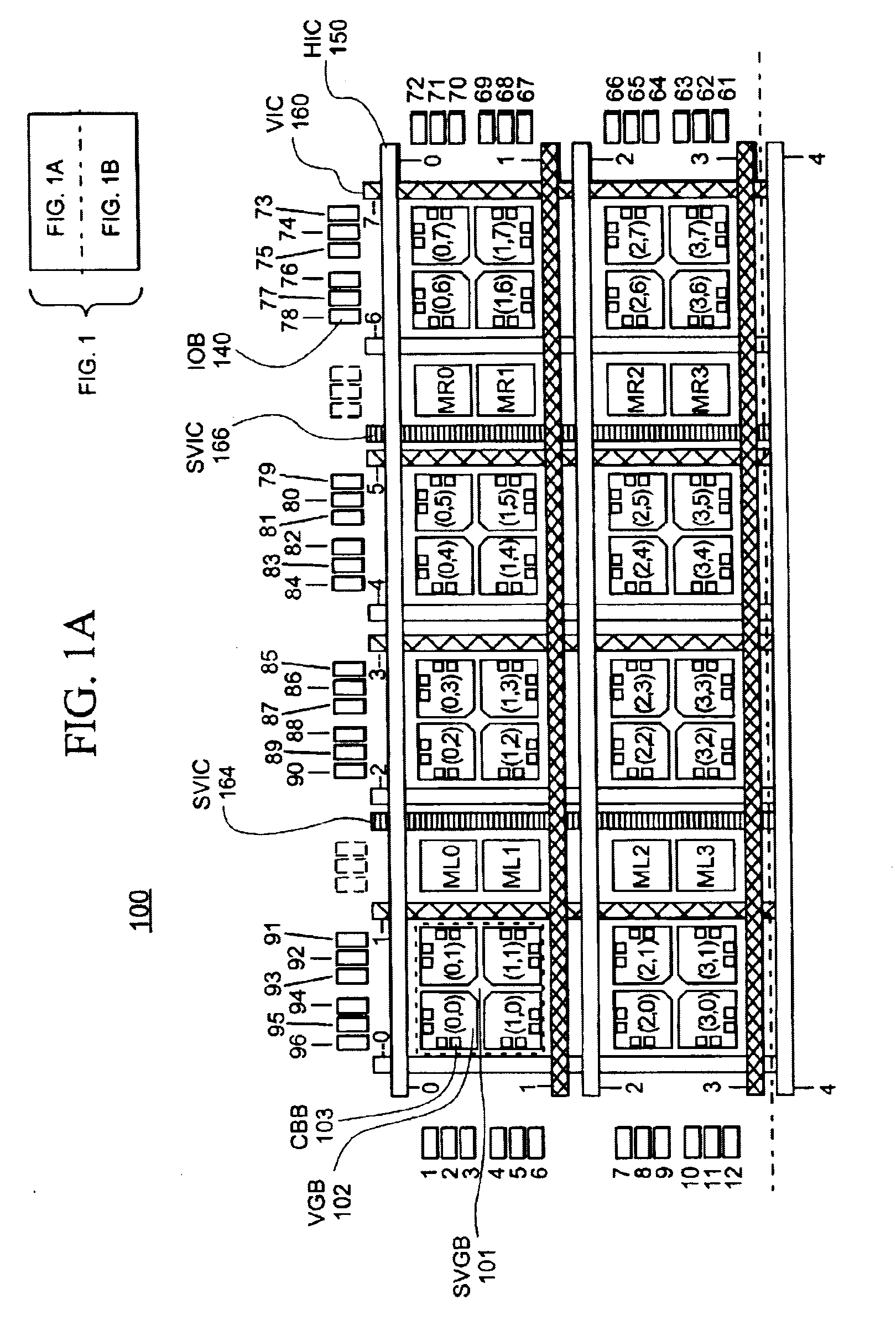
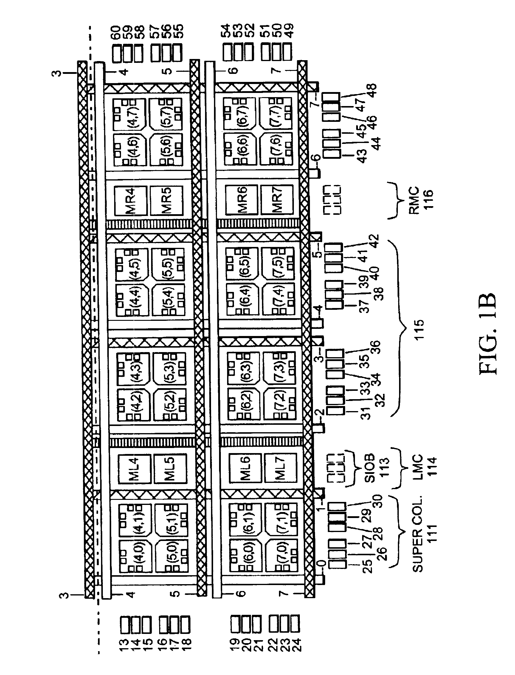
[0075]FIG. 1 shows a macroscopic view of an FPGA device 100 in accordance with the invention. The illustrated structure is preferably formed as a monolithic integrated circuit.

[0076]The macroscopic view of FIG. 1 is to be understood as being taken at a magnification level that is lower than later-provided, microscopic views. The more microscopic views may reveal greater levels of detail which may not be seen in more macroscopic views. And in counter to that, the more macroscopic views may reveal gross architectural features which may not be seen in more microscopic views. It is to be understood that for each more macroscopic view, there can be many alternate microscopic views and that the illustration herein of a sample microscopic view does not limit the possible embodiments of the macroscopically viewed entity. Similarly, the illustration herein of a sample macroscopic view does not limit the possible embodiments into which a microscopically viewed embodiment might be included.

[00...


PUM


Abstract

A field-programmable gate array device (FPGA) having plural rows and columns of logic function units (VGB's) further includes a plurality of embedded memory blocks, where each memory block is embedded in a corresponding row of logic function units. Each embedded memory block has a registered address port for capturing received address signals in response to further-received, address-validating clock signals. Interconnect resources are provided for conveying the address-validating clock signals to address-changing circuitry so that a next address can be generated safely in conjunction with the capturing by the registered address port of a previous address signal.

Description

CROSS REFERENCE TO RELATED APPLICATIONS[0001]The following copending U.S. patent applications are owned by the owner of the present application, and their disclosures are incorporated herein by reference:[0002](A) Ser. No. 08 / 948,306 filed Oct. 9, 1997 by Om P. Agrawal et al. and originally entitled, “VARIABLE GRAIN ARCHITECTURE FOR FPGA INTEGRATED CIRCUITS”;[0003](B) (A) Ser. No. 08 / 996,049 filed Dec. 22, 1997 by Om P. Agrawal et al and originally entitled, DUAL PORT SRAM MEMORY FOR RUN-TIME USE IN FPGA INTEGRATED CIRCUITS;[0004](C) Ser. No. 08 / 996,361 filed Dec. 22, 1997, by Om Agrawal et al. and originally entitled, “SYMMETRICAL, EXTENDED AND FAST DIRECT CONNECTIONS BETWEEN VARIABLE GRAIN BLOCKS IN FPGA INTEGRATED CIRCUITS”;[0005](D) Ser. No. 08 / 995,615 filed Dec. 22, 1997, by Om Agrawal et al. and originally entitled, “A PROGRAMMABLE INPUT / OUTPUT BLOCK (IOB) IN FPGA INTEGRATED CIRCUITS”;[0006](E) Ser. No. 08 / 995,614 filed Dec. 22, 1997, by Om Agrawal et al. and originally entitl...

Claims


Application Information

Patent Timeline
Patent Type & Authority Patents(United States)
IPC IPC(8): G06F7/38H03K19/177
CPCH03K19/17728H03K19/17736H03K19/17748H03K19/1776
Inventor AGRAWAL, OM P.CHANG, HERMAN M.SHARPE-GEISLER, BRADLEY A.NGUYEN, BAI
Owner LATTICE SEMICON CORP
Learn More