Flat panel display including electron emitting device

Inactive Publication Date: 2008-11-11
CANON KK
View PDF84 Cites 6 Cited by
  • Summary
  • Abstract
  • Description
  • Claims
  • Application Information

AI Technical Summary

Benefits of technology

[0020]The present invention was made to eliminate the disadvantages in the prior art as discussed above, and an object thereof is to provide an electron-emitting device that can have, without applying the treatment called forming, a quality more than equal to that of electron-emitting devices obtained by the forming, and has a novel structure suffering less irregularity of characteristics, and a method for preparing it.
[0021]More specifically, the present invention firstly provides a means for preparing the device by controlling the above-mentioned shape and width of cracks without use of the forming means, and with ease, and provides an electron-emitting device with regular characteristics, prepared by the method using the means.
[0023]A further object of the present invention is to provide an electron-emitting device capable of controlling the above characteristics and also capable of better controlling the position of the electron-emitting region, and a method for preparing such a device.
[0024]A still further object of the present invention is to provide an electric current emitting device that not only can solve the problems previously mentioned, but also can make lower the voltage to be applied to electrodes and achieve improvement in the density of an emitted electric current.

Problems solved by technology

However, the forming of the electron-emitting region according to the conventional energizing heat treatment as mentioned above havehas involved the problems as follows:(1) In carrying out the energizing heating, it sometimes occurs that the thin film is peeled because of the difference in a coefficient of thermal expansion between the substrate and the thin film.
This provides limitations in an upper limit of the heating temperature, materials for the substrate, and combination by selection of materials for the thin film.(2) In carrying out the energizing heating, the substrate also is locally heated, therefore sometimes resulting in occurrence of fatal cracking therein.(3) Degree of the changes of a film owing to the energizing heating, as exemplified by the degree of local destruction, deformation or denaturing, tends to become irregular among a plurality of devices formed in the same substrate, and also the site at which changes may occur tends to be not fixed.
For this reason, an electric source of large capacity is required when a number of devices are formed on the same substrate and the forming is carried out simultaneously.(5) A relatively long period of time is required for conventional forming processes that start with the energizing heating and end with cooling.
For this reason, an excessively long time is required for carrying out the forming of a number of devices.
Because of the problems as set out above, the surface conduction electron-emitting devices have not been positively applied in industrial fields, notwithstanding their advantages that the devices hashave simple constructions.

Method used


Image

  • Flat panel display including electron emitting device
  • Flat panel display including electron emitting device
  • Flat panel display including electron emitting device

Examples


example 1

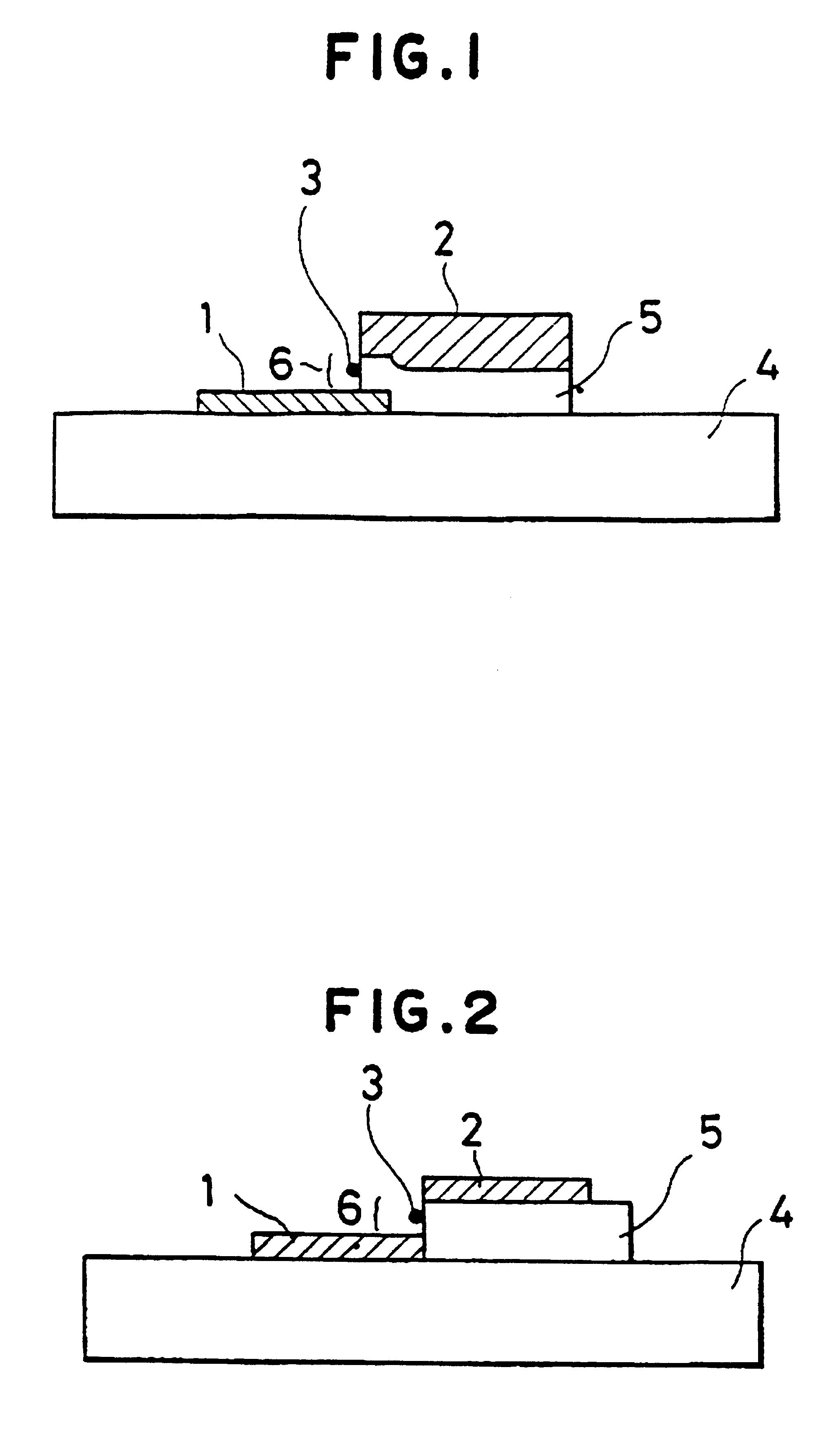
[0244]FIG. 3 (a), (b) is a flow sheet illustrating an example for a method of preparing the electron-emitting device of the present invention.

[0245]In FIG. 3(a), (b), the numeral 4 denotes a glass substrate; and 1, a nickel electrode of 500 angstroms thick.

[0246]SiO2 was vapor deposited to form an insulating layer 5a of 1,000 angstroms thick. Au was vapor deposited as an electron-emitting layer 3a to have a thickness of 500 angstroms, and an insulating layer 5b was also formed in the same manner as for 5a, thus bringing these three layers into lamination.

[0247]Then these were partly laminated on the electrode 1 as illustrated in FIG. 3 (a), along the pattern of the electrode 1, followed by patterning. Next, Ni was laminated as an electrode 2 with a film thickness of 5,000 angstroms.

[0248]As illustrated in FIG. 3 (b), the electrode 2 was subjected to patterning by usual photolithographic process along the patterns of the electrode 1, insulating layer 5a, electron-emitting layer 3a an...

example 2

[0251]In FIG. 4, the numerals 1 to 5 denote the same as in FIG. 3. In this figure, the numeral 8 denotes an intermediate layer, which is interposed between the insulating layer 5b and electrode 2 to contribute a multi-layer electrode. In the present Example, subsequent to the formation of the insulating layer 5b, a step to vapor-deposit LaB6 to a thickness of 1,000 angstroms followed by patterning was added to the preparation steps in Example 1. The electrode 2 was also formed by using Ni with a thickness of 5,000 angstroms as in Example 1.

[0252]Applying a voltage of 20 V between the electrode 2a and 2b of the device thus obtained, there was obtained emission of an electron beam 7 of 0.5 μA per 1 mm length of width of the electrode 2a in the direction vertical to the paper surface.

example 3

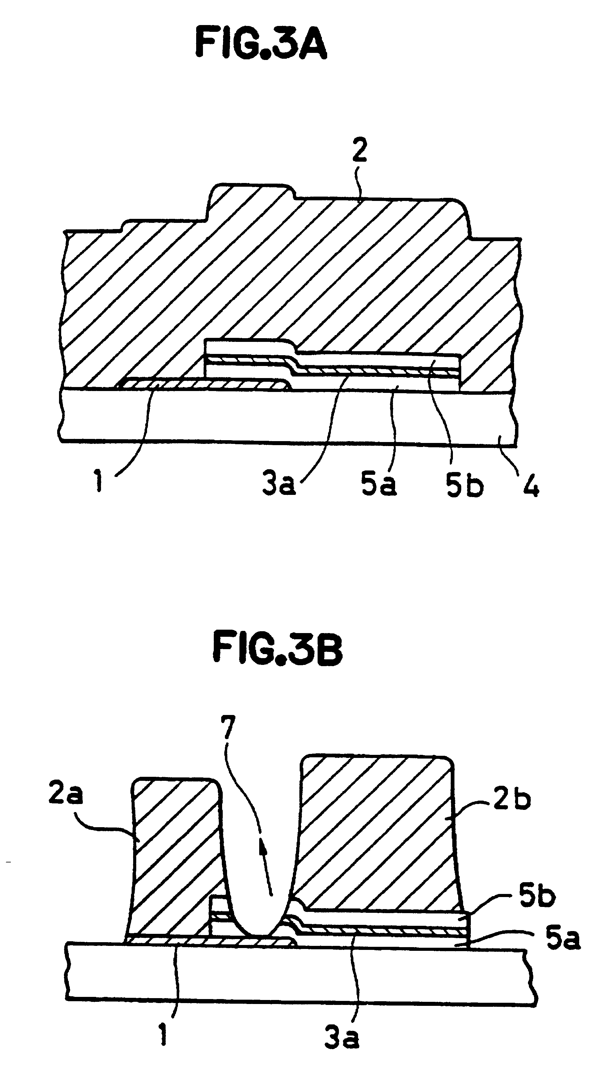
[0253]FIG. 6(a), (b) is a flow sheet illustrating an example for a method of preparing the electron-emitting device according to the second embodiment of the present invention. In FIG. 6 (a), (b), the numeral 4 denotes a glass substrate.

[0254]An insulating layer 5a was formed with SIO2 in 1,500 angstrom thickness; an electron-emitting layer 3a, with Pd in 250 angstroms thickness; and an insulating layer 5b, with SiO2 in 500 angstrom thickness, each of which layer was obtained by vacuum deposition and thereafter, as illustrated in FIG. 6 (a), etched to have a stepped shape to effect patterning. Next, electrodes 1 and 2 are deposited. The electrodes, as illustrated in FIG. 6 (b), are deposited on the insulating layer 5a and 8b and the stepped portion formed by the electron-emitting layer 3a with use of Ni with a thickness of 1,000 angstroms. In this occasion, generally the electrode 1 will not come into contact with the electron-emitting layer 3 if the thickness of the electrode is ma...


PUM


Abstract

A display device consisting of an electron-emitting device which is a laminate of an insulating layer and a pair of opposing electrodes formed on a planar substrate. A portion of the insulating layer is between the electrodes and a portion containing an electron emitting region in between one electrode and the substrate. Electrons are emitted from the electron emission region by a voltage to the electrodes, thereby stimulating a phosphorous to emitting light.

Description

RELATED APPLICATION[0001]This application is a reissue of U.S. Pat. No. 5,661,362, which issued on Aug. 26, 1997 from application Ser. No. 08 / 657,385 filed Jun. 3, 1996, which is a continuation of application Ser. No. 08 / 396,066 filed Feb. 28, 1995, now abandoned, which is a continuation of application Ser. No. 08 / 191,065 filed Feb. 3, 1994, now abandoned, which is a continuation of application Ser. No. 07 / 705,72107 / 705,720filed May 24, 1991, abandoned, which is a continuation-in-part of application Ser. No. 07 / 218,203 filed Jul. 13, 1988 and issued as U.S. Pat. No. 5,066,883 on Nov. 19, 1991.BACKGROUND OF THE INVENTION[0002]1. Field of the Invention[0003]The present invention relates to an electron-emitting device, and a method of preparing it.[0004]2. Related Background Art[0005]Hitherto known as a device achievable of emission of electrons with use of a simple structure is the cold cathode device published by M. I. Elinson et al (Radio Eng. Electron. Phys., Vol. 10, pp.1290-1296,...

Claims


Application Information

Patent Timeline
IPC IPC(8): H01J1/30G09G3/20
CPCH01J29/04H01J31/127
Inventor YOSHIOKA, SEISHIRONOMURA, ICHIROSUZUKI, HIDETOSHITAKEDA, TOSHIHIKOKANEKO, TETSUYABANNO, YOSHIKAZUYOKONO, KOJIRO
Owner CANON KK
Why Eureka
Try Eureka