
Semiconductor device

a technology of semiconductors and devices, applied in solid-state devices, basic electric elements, foundation engineering, etc., to prevent the strength of wire bonding from dropping

Active Publication Date: 2010-10-19
III HLDG 12 LLC
View PDF27 Cites 5 Cited by
  • Summary
  • Abstract
  • Description
  • Claims
  • Application Information

AI Technical Summary

Benefits of technology

The present invention provides a semiconductor device that prevents damage to function elements and maintains wire bonding strength. It achieves this by using an interposer chip with connection wirings that are connected to an externally leading electrode on a semiconductor chip through wire bonding. This eliminates the need for a rewiring layer that can deteriorate the electric property of the semiconductor chip and decrease the connection strength in wire bonding. The interposer chip also prevents damage to the underlying wirings and improves the overall wire bonding strength.

Problems solved by technology

Thus, it is possible to suppress such a problem that: the wire becomes brittle when the wire is long, and the wire hangs down due to its weight, which causes the wire to touch another wire and causes the wire to touch an edge of the lower semiconductor chip.

Method used


Image

  • Semiconductor device
  • Semiconductor device
  • Semiconductor device

Examples


embodiment 1

[Embodiment 1]

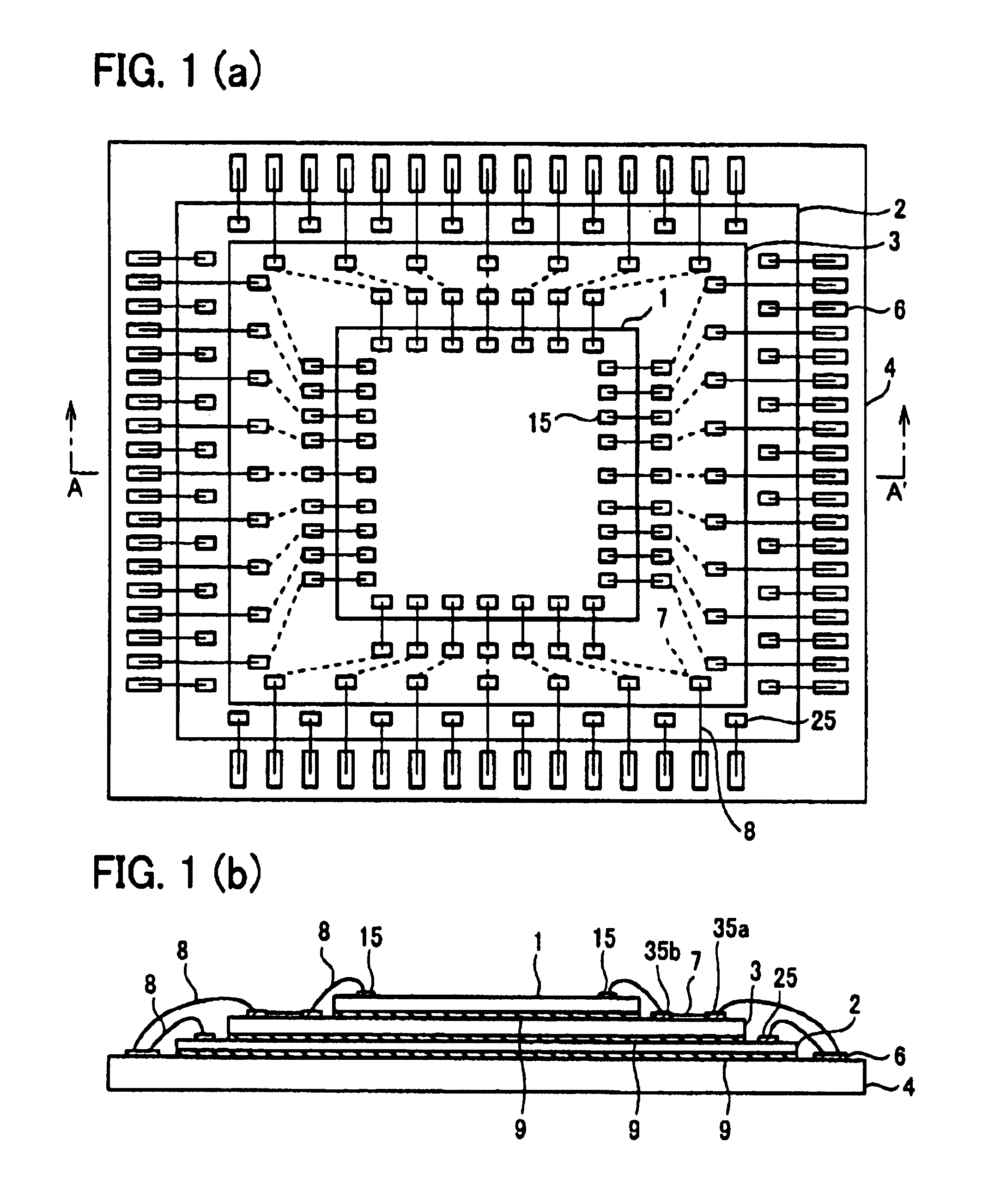
[0043]The following description will explain one embodiment of the semiconductor device of the present invention with reference to FIG. 1(a) and FIG. 1(b). Note that, the present invention is not limited to this.

[0044]FIG. 1(a) is a plan view obtained by viewing the semiconductor device of the present embodiment from above in a stacking direction, and FIG. 1(b) is a cross sectional view taken along A-A′ of FIG. 1(a).

[0045](Structure of the Semiconductor Device)

[0046]As shown in FIG. 1 (a) and FIG. 1 (b), the semiconductor device of the present embodiment is arranged so that: a substrate 4 is used as a stacking base, and a semiconductor chip 2, an interposer chip 3, and a semiconductor chip 1 are stacked on and above the stacking base in this order. Note that, by using die-bonding layers 9, the substrate 4 and the semiconductor chip 2 are bonded to each other, and the semiconductor chip 2 and the interposer chip 3 are bonded to each other, and the interposer chip 3 and ...

embodiment 2

[Embodiment 2]

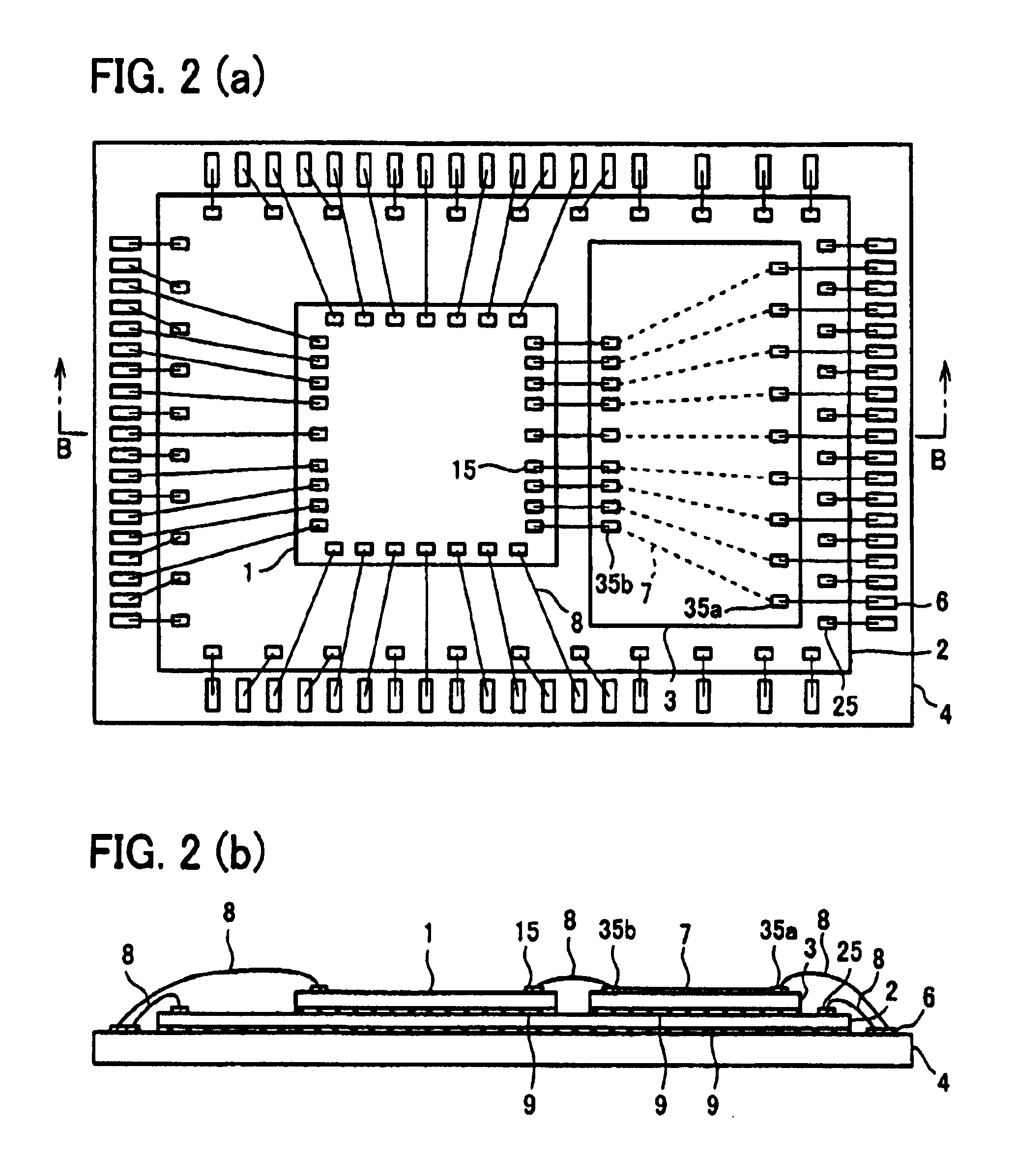
[0064]The following description will explain another embodiment of the semiconductor device of the present invention with reference to FIG. 2(c) and FIG. 2(b). Note that, for convenience in description, same reference signs are given to members having the same function as members described in Embodiment 1, and description thereof is omitted.

[0065]FIG. 2(a) is a plan view obtained by viewing the semiconductor device of the present embodiment from above in a stacking direction, and FIG. 2(b) is a cross sectional view taken along B-B′ of FIG. 2(b). As shown in FIG. 2(a) and FIG. 2(b), the semiconductor device of the present embodiment is arranged so that: the semiconductor chip 2 is stacked on an upper surface of the substrate 4, and the semiconductor chip 1 and the interposer chip 3 are stacked thereon so as to be positioned side by side. Note that, by using die-bonding layers 9, the substrate 4 and the semiconductor chip 2 are bonded to each other, and the semiconductor...

embodiment 3

[Embodiment 3]

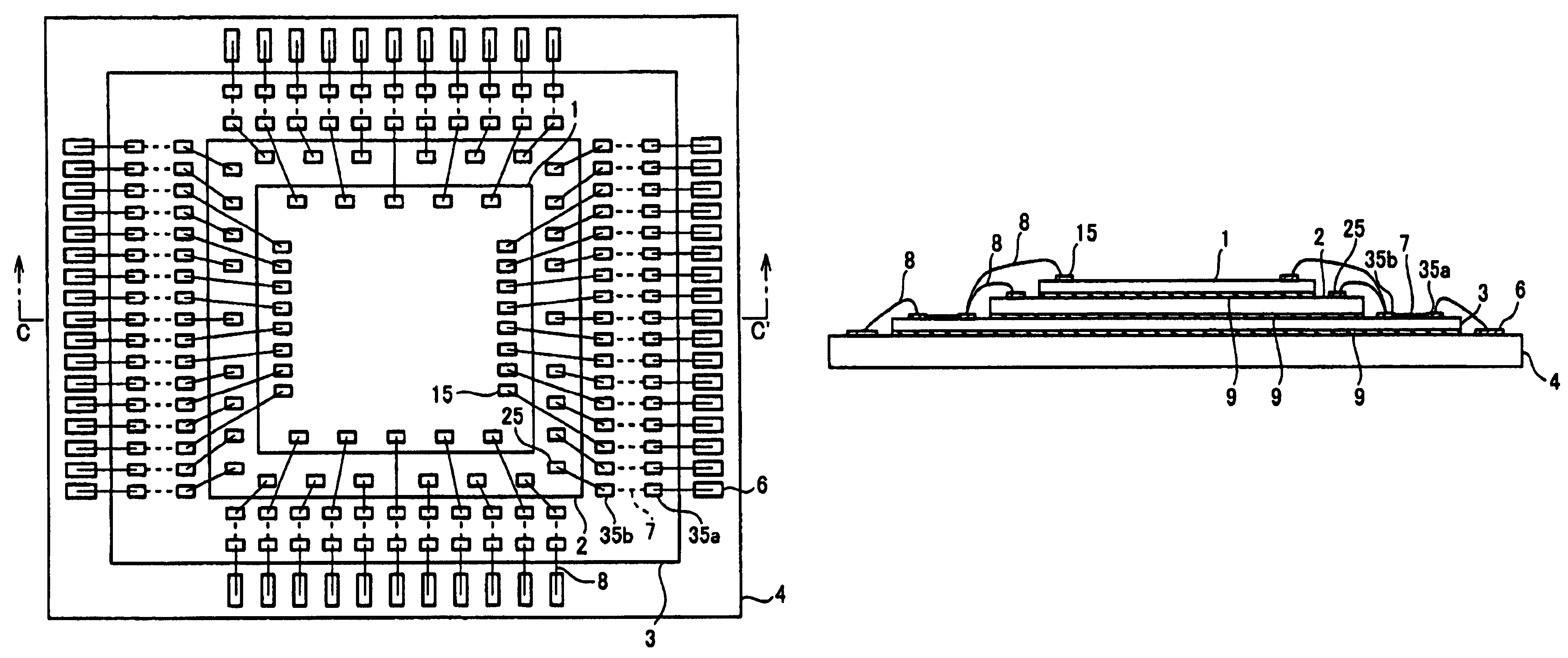
[0072]The following description will explain still another embodiment of the semiconductor device of the present invention with reference to FIG. 3(a) and FIG. 3(b). Note that, for convenience in description, the same reference signs are given to members having the same functions as members described in Embodiment 1, and description thereof is omitted.

[0073]FIG. 3(a) is a plan view obtained by viewing the semiconductor device of the present embodiment from above in a stacking direction, and FIG. 3(b) is a cross sectional view taken along C-C′ of FIG. 3(a). As shown in FIG. 3(a) and FIG. 3(b), the semiconductor device of the present embodiment is arranged so that: the interposer chip 3 is stacked on an upper surface of the substrate 4, and the semiconductor chips 1 and 2 are stacked thereon and thereabove in this order. That is, in the present embodiment, the interposer chip 3 is formed between the substrate 4 and the semiconductor chip 2.

[0074]The bonding pads 15 . . ....


PUM


Abstract

In a semiconductor device in which a semiconductor chip is stacked on a substrate, an interposer chip having wirings is provided under the semiconductor chip. A bonding pad of the semiconductor chip is electrically connected to a bonding terminal provided on the substrate via the interposer chip by wire bonding. The interposer chip prevents a semiconductor element formed in the semiconductor chip from deteriorating in terms of an electric property and from being physically damaged. Further, the wire bonding strength does not drop. Moreover, it is possible to form a fine wiring pitch for relaying a wire-bonding wire.

Description

[0001]This Nonprovisional application claims priority under 35 U.S.C. §119(a) on Patent Application No. 2003 / 020971 filed in Japan on Jan. 29, 2003, the entire contents of which are hereby incorporated by reference.FIELD OF THE INVENTION[0002]The present invention relates to a semiconductor device, particularly, to a semiconductor device in which a plurality of semiconductor chips are stacked.BACKGROUND OF THE INVENTION[0003]In order to realize high-density installation of semiconductor chips which is a key technology for making an electronic device smaller, lighter, and thinner, various packaging techniques of a semiconductor device have been developed.[0004]As a technique concerning a packaging structure of a semiconductor device which reduces an area required in installing the semiconductor device onto a mother board, there have been developed: a pin-insert package such as DIP (Dual Inline Package); a surface installation package, such as SOP (Small Outline Package), performed by...

Claims


Application Information

Patent Timeline
Patent Type & Authority Patents(United States)
IPC IPC(8): H01L23/48H01L25/18H01L21/52H01L21/60H01L23/12H01L25/065H01L25/07
CPCH01L24/49H01L25/0657H01L23/49838H01L24/29H01L2224/32225H01L2924/19107H01L2924/15173H01L2924/01082H01L2924/01079H01L2924/01033H01L2924/01014H01L2924/01013H01L2924/01006H01L2924/01005H01L2924/01004H01L2225/06572H01L2225/06555H01L2225/06527H01L2225/0651H01L24/45H01L2224/32145H01L2224/45124H01L2224/45144H01L2224/48091H01L2224/48137H01L2224/48145H01L2224/48157H01L2224/48227H01L2224/4846H01L2224/49171H01L2224/49175H01L2225/06506H01L2924/00014H01L2924/00H01L2924/3512H01L2224/05553H01L2224/73265H01L24/48H01L2224/023H01L2924/00012H01L2924/0001E02D5/72
Inventor NISHIDA, HISASHIGESOTA, YOSHIKIJUSO, HIROYUKI
Owner III HLDG 12 LLC
Learn More