Input buffer circuit for stabilizing logic converting point
An input buffer, logic conversion technology, applied in the direction of logic circuit connection/interface layout, logic circuit coupling/interface using field effect transistors, etc., can solve the problems of signal conversion error, CMOS circuit failure, noise margin deterioration, etc.
- Summary
- Abstract
- Description
- Claims
- Application Information
AI Technical Summary
Problems solved by technology
Method used
Image

Examples
Embodiment Construction
[0060] Embodiments of the present invention will now be described with reference to the accompanying drawings.
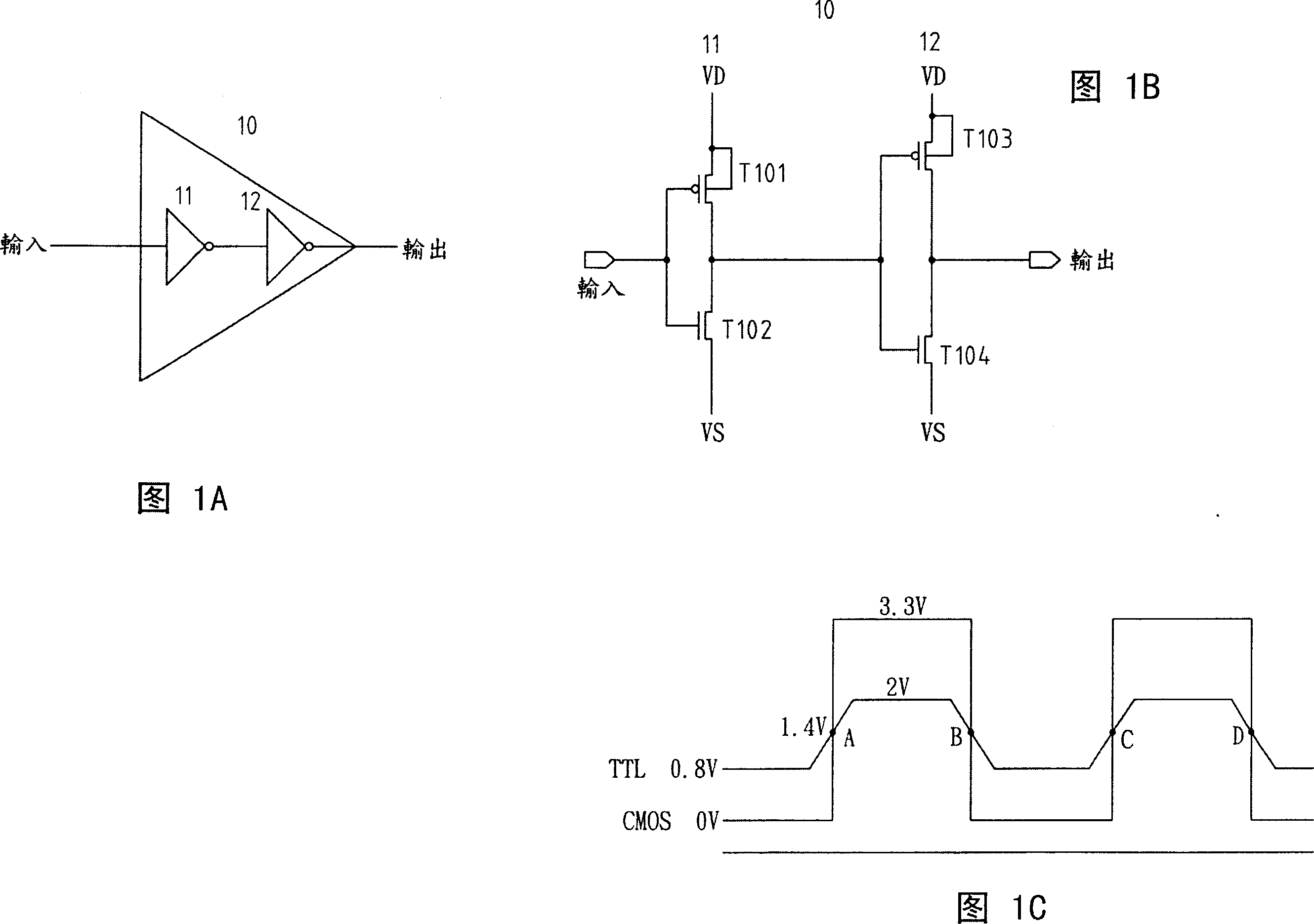
[0061] First, please refer to FIGS. 4A and 4B , which show a circuit structure diagram of the input buffer 40 converted from TTL to CMOS according to the present invention. Among them, FIG. 4A is a functional block diagram of the circuit, and FIG. 4B is a detailed diagram of the circuit structure.
[0062] It can be seen from FIG. 4A that the buffer 40 is composed of a first inverting stage 41 , a second inverting stage 42 , and a bias voltage 43 . Please refer to FIG. 4B, which shows a detailed circuit diagram of an input buffer converted from TTL to CMOS according to an embodiment of the present invention, which includes:
[0063] The input buffer 40, which receives the voltage input by TTL, converts it into an appropriate level voltage and outputs it to supply the CMOS circuit, including:
[0064] The first inverter stage 41, which is an input stage, receives t...
PUM
 Abstract
Description
Claims
Application Information
 - R&D
- Intellectual Property
- Life Sciences
- Materials
- Tech Scout
- Unparalleled Data Quality
- Higher Quality Content
- 60% Fewer Hallucinations
Browse by: Latest US Patents, China's latest patents, Technical Efficacy Thesaurus, Application Domain, Technology Topic, Popular Technical Reports.
© 2025 PatSnap. All rights reserved.Legal|Privacy policy|Modern Slavery Act Transparency Statement|Sitemap|About US| Contact US: help@patsnap.com