Direct calculation method of interface trap in MOS semiconductor field-effect rransistor

A technology of interface defects and measurement methods, applied in semiconductor/solid-state device testing/measurement, semiconductor characterization, single semiconductor device testing, etc.

Inactive Publication Date: 2008-03-26
UNITED MICROELECTRONICS CORP
View PDF5 Cites 0 Cited by
  • Summary
  • Abstract
  • Description
  • Claims
  • Application Information

AI Technical Summary

Problems solved by technology

However, this method is still affected by DTGL
When the gate oxide thickness is reduced to the direct tunneling range (t ox <30 angstroms), especially in the measurement of 16 angstroms ultra-thin gate oxide interface defects, so far there is no CP method that can accurately, quickly and effectively obtain satisfactory measurement results; let alone 12 angstroms The ultra-thin gate oxide layer below

Method used


Image

  • Direct calculation method of interface trap in MOS semiconductor field-effect rransistor
  • Direct calculation method of interface trap in MOS semiconductor field-effect rransistor
  • Direct calculation method of interface trap in MOS semiconductor field-effect rransistor

Examples


Embodiment Construction

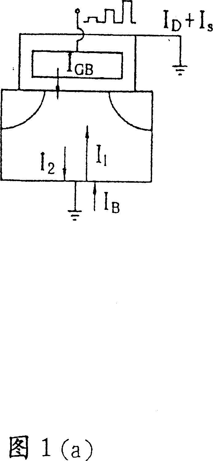
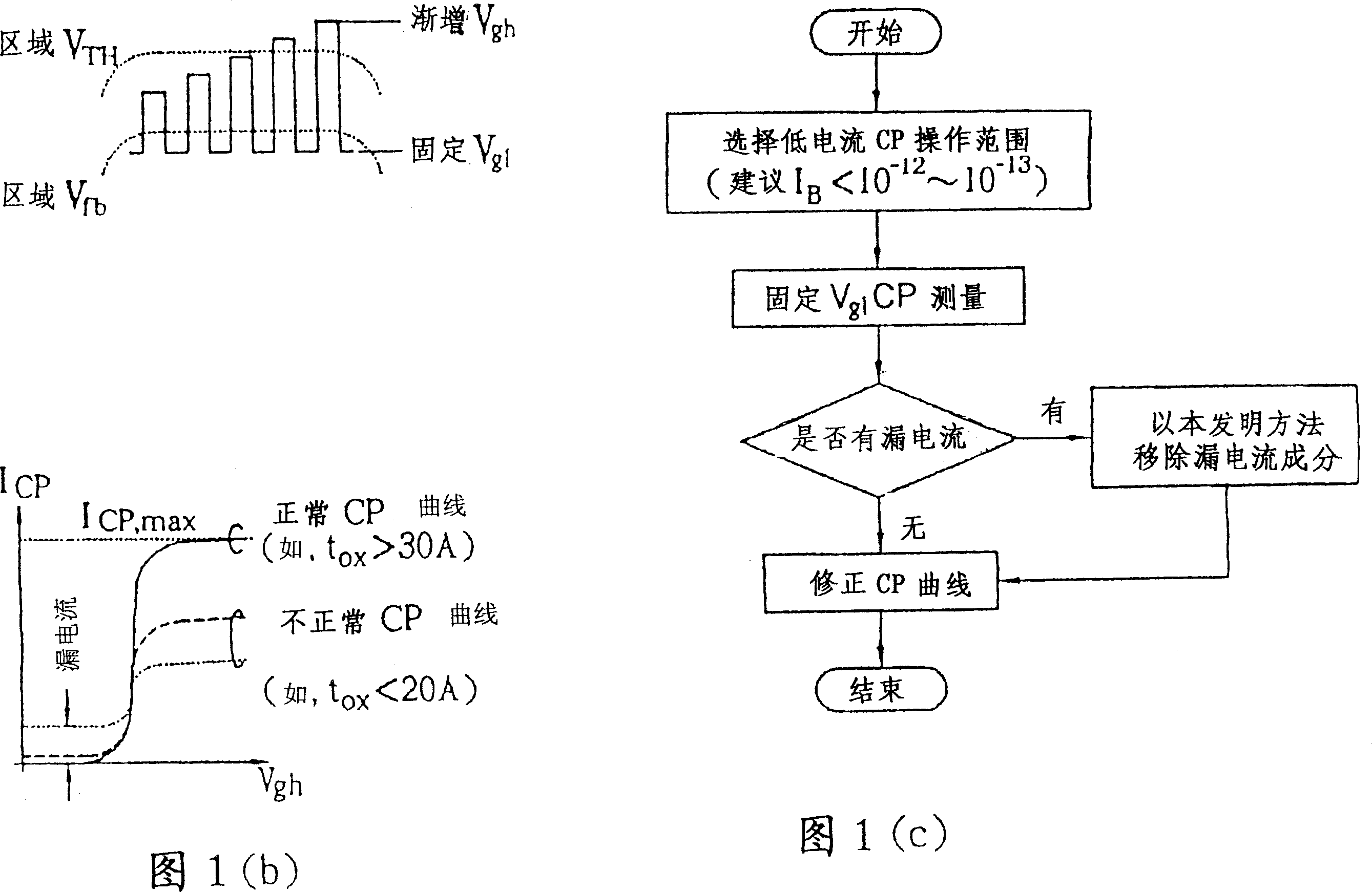
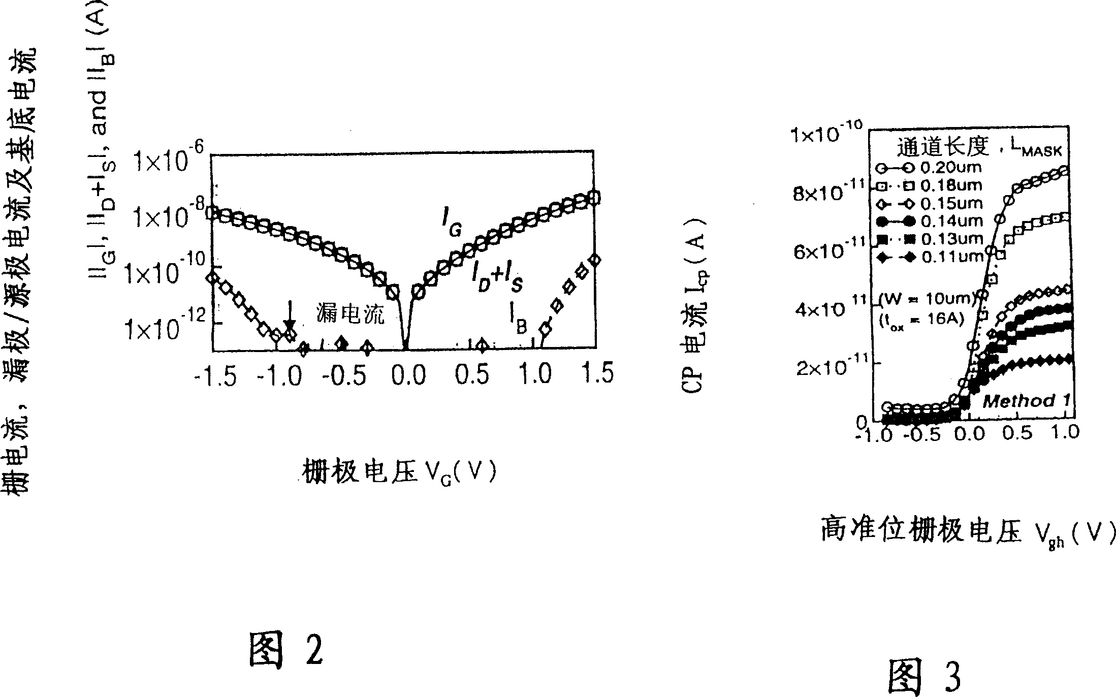
[0028] The present invention provides a method for directly and accurately calculating gate oxide layer interface defects (interface traps, hereinafter referred to as N for short) of advanced MOSFET components. it ) method of quantity. The so-called advanced MOSFET device generally refers to a very short channel length (e.g., actual gate length (L gate ) can be less than 1 micron) and an ultra-thin gate oxide layer with a tunneling leakage effect (e.g., t ox 2 -10 3 order of magnitude tunneling leakage current. In order to make this advanced nanoscale device, photoresist exposure and removal techniques are used, which makes the actual gate length (L gate ) will be longer than the mask exposure length (L mask ) is about 0.04 microns; the actual gate length is designed to be 0.07-0.18 microns. (Note: Of course, this method can also be applied to components whose actual gate length is greater than 1 micron.)

[0029] Please refer to Figure 1(a). This figure discusses the ar...


PUM


Abstract

A method which is used for directly calculating the defect amount of the metal-oxide half field-effect transistor which mainly comprises the following procedures: (1) constructing a measuring interval suitable for the low electric leakage to find out a given interval which can be suitable for the bias voltage (Vgl and Vgh) of the grid impulse (gate pulse); (2) eliminating the parasitical tunneling drain current with a low drain current CP method, and a high-low frequency measuring method or frequency adding CP measuring method can be adopted; the present invention uses the low electric leakage CP method to eliminate the considerable parasitic drain current and can be accurately applied for calculating the interface defect of the grid oxidizing layer and effectively evaluating the grid oxidizing layer growing quality / oxidizing layer technique; the experiment data shows that the analysis relative to the interface defect of the grid oxidizing layer, such as the generation of the grid interface defect, the monitoring to the grid oxidizing layer thin film and the evaluating to the reliability of the microminiature CMOS element, the invention can calculate the number of the interface defect (Nit) quickly and simply and the satisfactory result can be obtained.

Description

[0001] (The present invention is a divisional application, the original application number is 03100292.7, the application date is January 10, 2003, and the title of the invention is "Method for Directly Calculating the Defect Quantity at the Interface of Metal Oxide Semiconductor Field Effect Transistor") technical field [0002] The present invention relates to a semiconductor wafer testing method, in particular to an accurate and fast method for calculating the number of gate oxide interface defects (interface traps) in metal oxide semiconductor field effect transistor (MOSFET) elements. This method can provide such as the measurement of the number of gate oxide layer interface defects, the monitoring of the gate oxide layer film quality, the effective physical channel length of components, the evaluation of the reliability of ultra-small components, etc., any detection related to gate oxide layer interface defects analyze. Background technique [0003] In recent years, se...

Claims


Application Information

Patent Timeline
Patent Type & Authority Patents(China)
IPC IPC(8): H01L21/66G01R31/26G01R31/28
CPCG01R31/2621G01R31/2831G01R31/2648
Inventor 庄绍勋陈尚志杨健国吴德源
Owner UNITED MICROELECTRONICS CORP
Why Eureka
Try Eureka