
Wafer laser marker method

A laser marking and laser marking technology, which is applied in the manufacturing of electrical components, electrical solid-state devices, semiconductor/solid-state devices, etc., and can solve the problem that the wafer cannot be laser marked.

Inactive Publication Date: 2008-06-25
CHIPMOS TECH INC
View PDF4 Cites 0 Cited by
  • Summary
  • Abstract
  • Description
  • Claims
  • Application Information

AI Technical Summary

Problems solved by technology

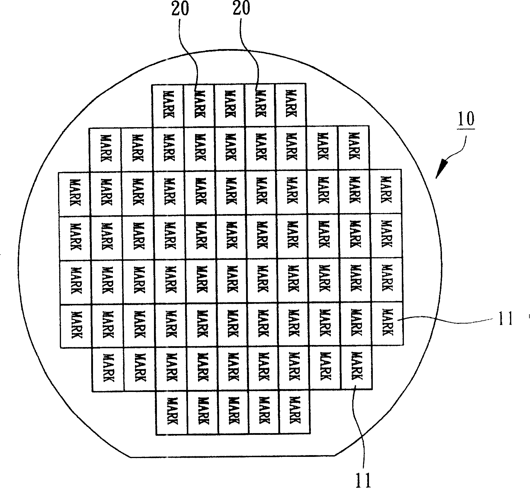
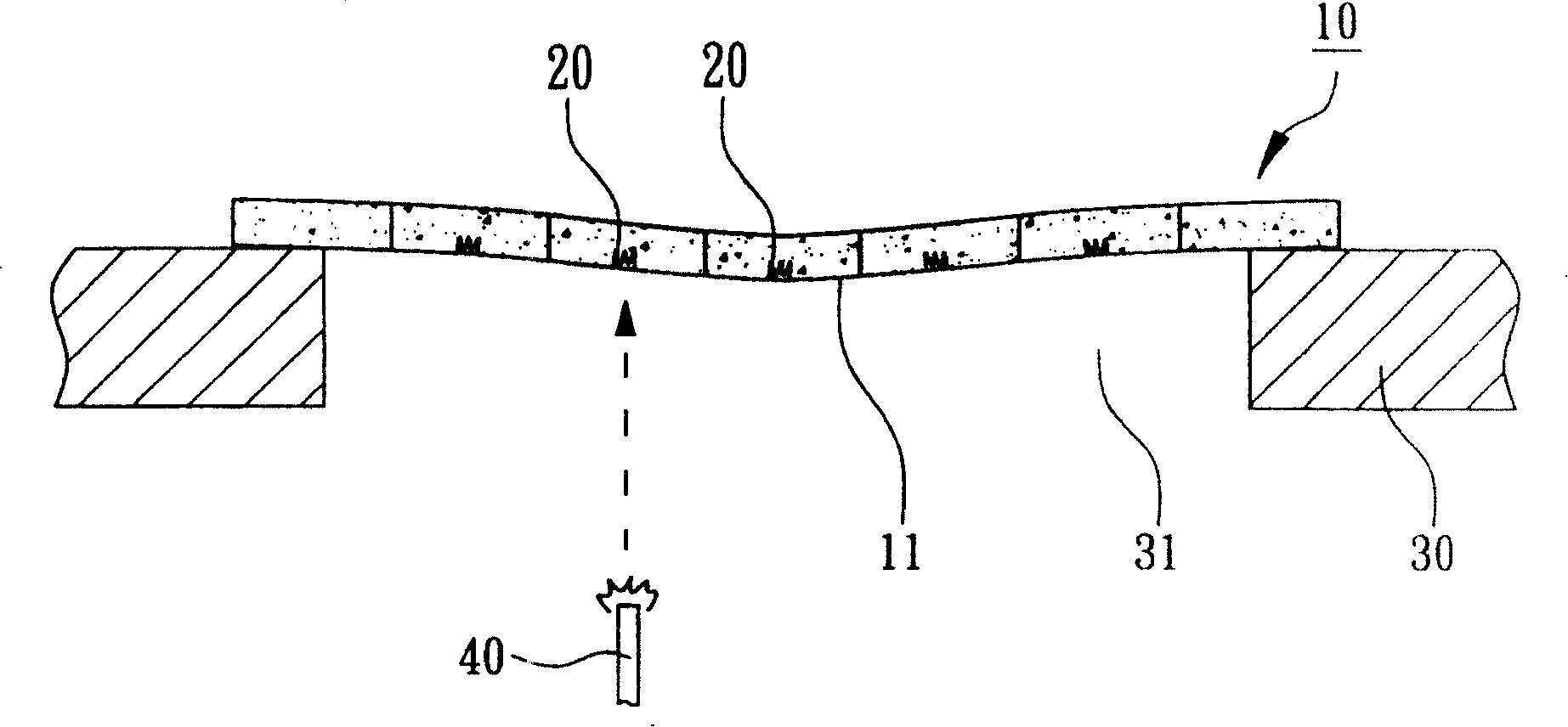
[0006] The main purpose of the present invention is to overcome the defects existing in the laser marking method of wafers, and provide a new laser marking method for wafers. The technical problem to be solved is to make it possible in a thinning (wafer Laser marking can be formed on wafers with a thickness ranging from 1 to 12 mils, which can solve the problem that thinned wafers cannot be laser marked, making it more suitable for practical use

Method used


Image

  • Wafer laser marker method
  • Wafer laser marker method
  • Wafer laser marker method

Examples


Embodiment Construction

[0043] In order to further explain the technical means and effects of the present invention to achieve the intended purpose of the invention, the following in conjunction with the accompanying drawings and preferred embodiments, the laser marking method for wafers proposed according to the present invention and its specific implementation methods, The method, steps, features and effects thereof are described in detail below.

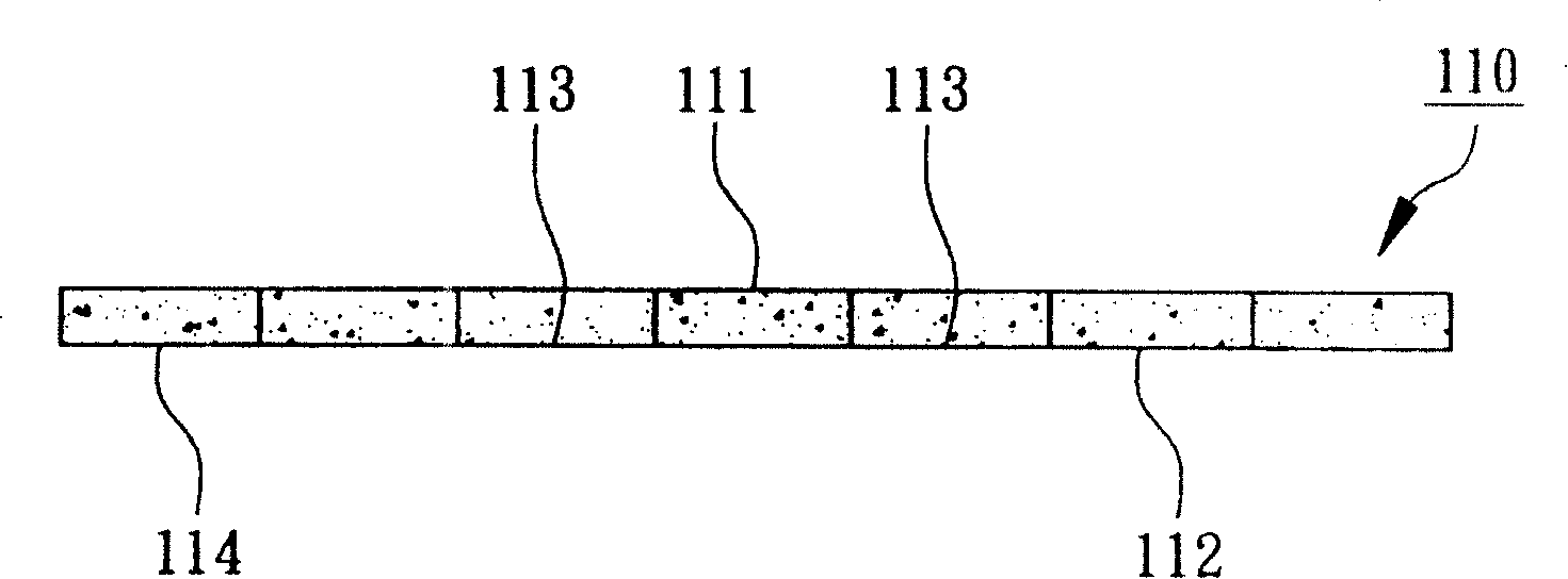
[0044] see image 3 Shown is a schematic cross-sectional view of a wafer provided according to a specific embodiment of the present invention. Firstly, a wafer 110 is provided. The wafer 110 includes a plurality of dies and has an active surface 111 and a back surface 112 . Various integrated circuits, pads and protection layers (not shown) are formed on the active surface 111 corresponding to each die area. see again image 3 and Figure 5 , the backside 112 of the wafer 110 includes a plurality of die backsides 113 and a die-free peripheral region ...


PUM


Abstract

The invention relates to a laser mark method of crystal chip and relative crystal chip. Wherein, it comprises: providing a crystal chip on the transmission carrier, while its back contacts parallel the carrier; when there is laser mark, the laser passes the transparent carrier to emit the back of crystal, to form at least one laser mark. The inventive crystal has one active surface and one back surface, while the thickness between them is 1-12mil, and the back surface has at least one laser mark.

Description

technical field [0001] The invention relates to a laser marking method of a wafer and the wafer thereof, in particular to a laser marking method of the wafer on the back side of the thinned wafer and the wafer thereof. Background technique [0002] Integrated circuit products are integrated and mass-produced on a wafer (wafer), and then cut into individual dies (die, or chip) for subsequent packaging or assembly operations. Due to the variety of integrated circuits, laser marks are usually made on the back of the die, such as various letters or numbers, to facilitate easy identification of the chip type or batch number. Related technologies can be found in China Taiwan Patent Announcement No. 395041 "Laser Marked Chip". A plurality of transistor elements are formed on the front side (ie, the active surface) of a crystal grain, and a laser mark is formed on the back side of the crystal grain as the crystal grain identity. Identification. [0003] At present, the production ...

Claims


Application Information

Patent Timeline
Patent Type & Authority Patents(China)
IPC IPC(8): H01L21/00H01L23/544
Inventor 苏淑玲陈光辉
Owner CHIPMOS TECH INC
Learn More