
Emission spectrometer having charge coupled device detector

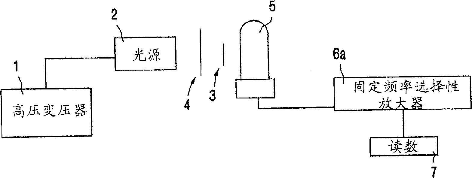
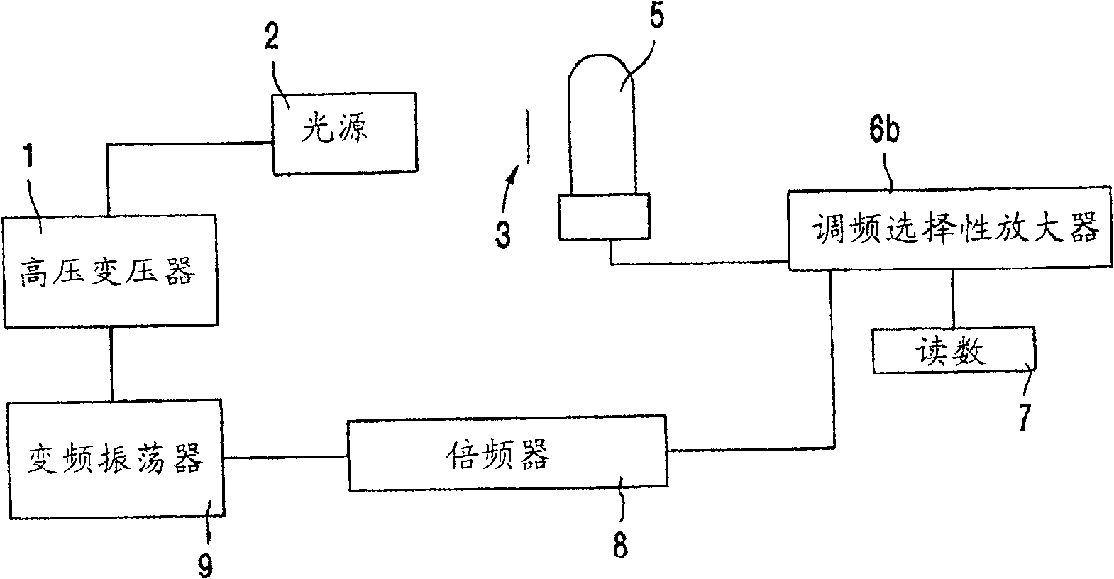
A technology of charge-coupled devices and emission spectroscopy, applied in the field of analyzers, can solve problems such as long-term baseline drift, difficulty in distinguishing changes in background light intensity, and increased cost, size, and complexity of analyzers

Inactive Publication Date: 2008-09-03
PRAXAIR TECH INC
View PDF8 Cites 0 Cited by
  • Summary
  • Abstract
  • Description
  • Claims
  • Application Information

AI Technical Summary

Problems solved by technology

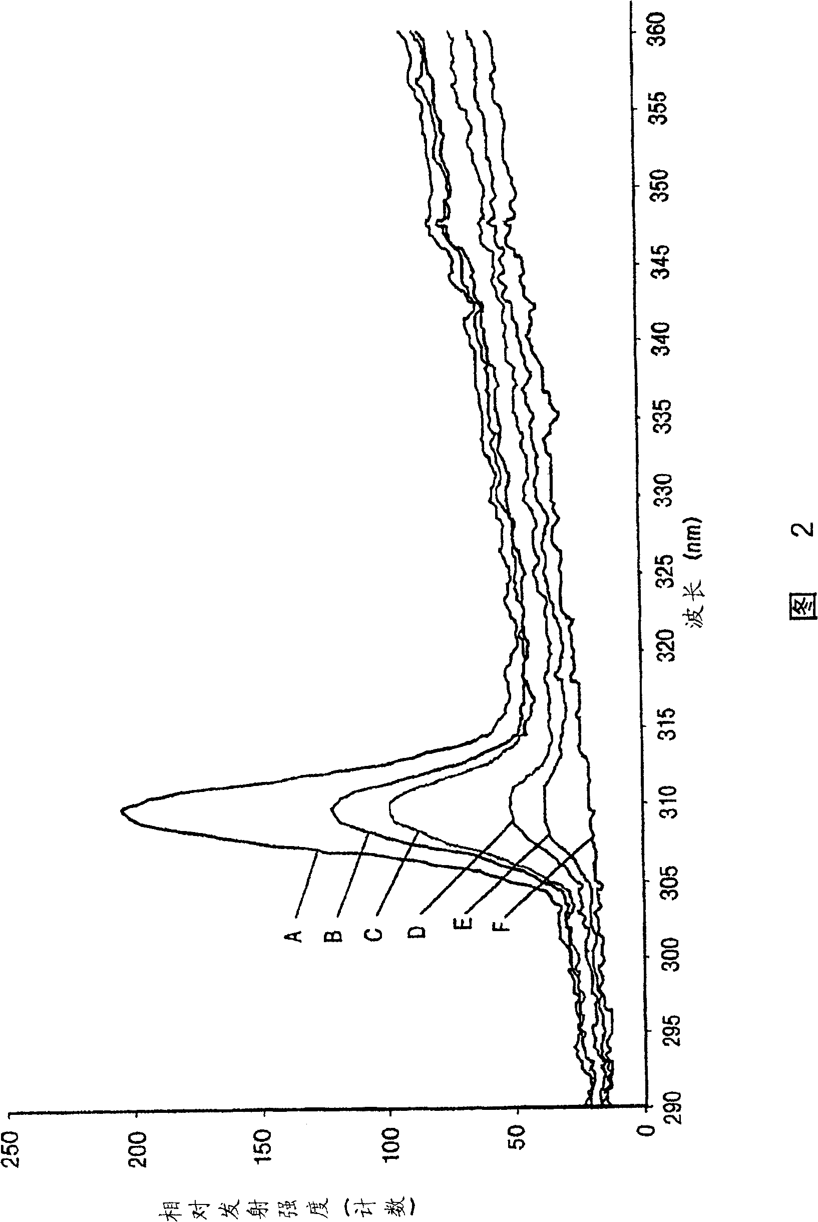
Distinguishing changes in background light intensity from changing impurity concentrations of interest is very difficult when only the emission intensity at the wavelength of interest is known
Variations in background light intensity can cause many problems: long-term baseline drift, non-linear calibration curves, and cross-sensitivity to other impurities
This can significantly increase the cost, size and complexity of the analyzer

Method used


Image

  • Emission spectrometer having charge coupled device detector
  • Emission spectrometer having charge coupled device detector
  • Emission spectrometer having charge coupled device detector

Examples


Embodiment Construction

[0035] DETAILED DESCRIPTION OF THE PREFERRED EMBODIMENT

[0036] Preferred embodiments of the apparatus and method of the present invention will be described with reference to the accompanying drawings.

[0037] Referring to FIG. 3 , it is a structural diagram of an exemplary analyzer using a CCD array emission spectrometer, which is a preferred embodiment of the present invention. Of course, other configurations using CCD array emission spectrometer elements can also be used. The analyzer in FIG. 3 includes spectrometer 10 , onboard computer 20 , analog and digital interface 30 , analytical sample cell 40 , transformer 50 , transformer basic input / input module 60 , power input module 70 and DC power supply 80 .

[0038] During operation, a gas sample to be analyzed is placed in the analytical sample cell 40 . A preferred sample system is the Praxair microcell, which is described in US Patent No. 6,043,881, which is hereby incorporated by reference. The advantages of the si...


PUM


Abstract

An analyzer suitable for performing continuous gas analysis in ultra-high purity applications. The analyzer combines a low-level emission source and a gaseous emission spectrometer (10) having a charge coupled device (CCD) diode array as a detector. The CCD detector replaces one or more photomultipliers and narrow bandpass filters typically used in spectrometers. The analyzer performs various processing operations to evaluate and eliminate the effect of background light level, or dark spectrum.

Description

technical field [0001] In general, the present invention relates to an emission spectrometer based analyzer with charge coupled devices for ultra high purity gas analysis. technical background [0002] Gas emission spectroscopy has been used for many years to analyze the nitrogen content of argon (see, eg, US Patent No. 3,032,654). The emission source commonly used for this technique is a low-energy argon plasma, also known as a silent discharge (SED). Over the years, this technique has been refined to reduce the limit of detection (LOD) to a single part per billion (ppb) level; for example by using electro-optical modulation (see eg US Patent No. 5,412,467). Further improvements in cell design, electronics, and microprocessor platforms have led to contemporary spectroscopic analyzers. Current practice using multiple detectors and filters allows simultaneous analysis of multiple impurities if the appropriate emission wavelengths can be found. [0003] The block diagram in...

Claims


Application Information

Patent Timeline
Patent Type & Authority Patents(China)
IPC IPC(8): G01J3/30G01N21/67G01J3/28G01J3/443G01N21/03G01N21/27
CPCG01J3/2803G01J3/443G01J3/30
Inventor M·L·马尔楚斯基J·韦格尔兹恩W·D·马丁
Owner PRAXAIR TECH INC
Learn More