

Active component array substrate and method for repairing its picture element unit
An active element and array substrate technology, which is applied to the field of repairing active element array substrates and their pixel units, can solve problems such as the formation of bright spots in pixel units, and achieve the effect of avoiding bright spots.
- Summary
- Abstract
- Description
- Claims
- Application Information
AI Technical Summary
Problems solved by technology
Method used
Image

Examples
no. 1 example
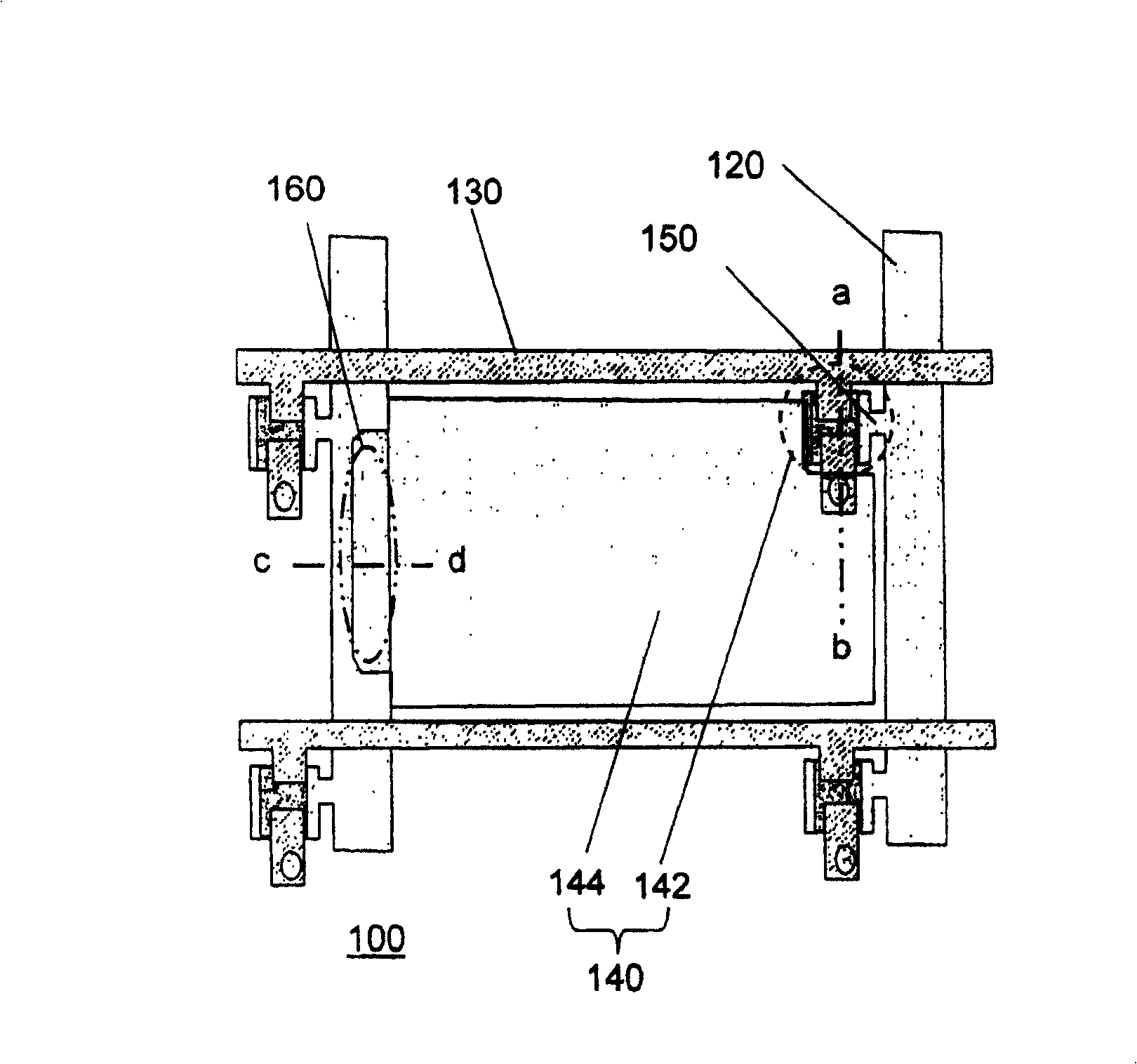
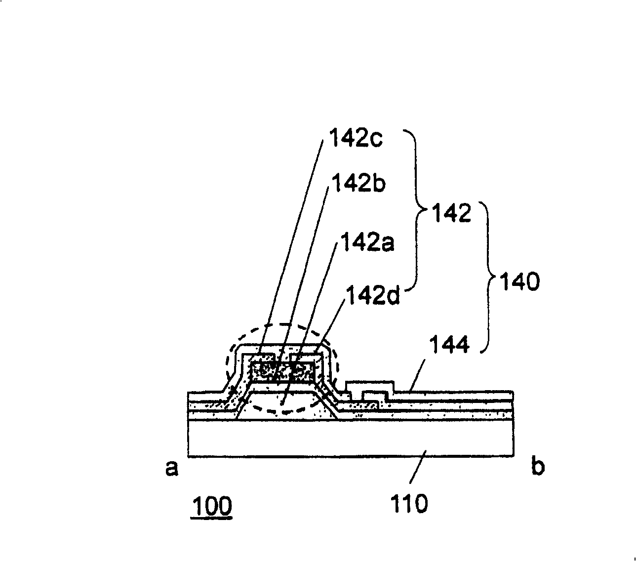
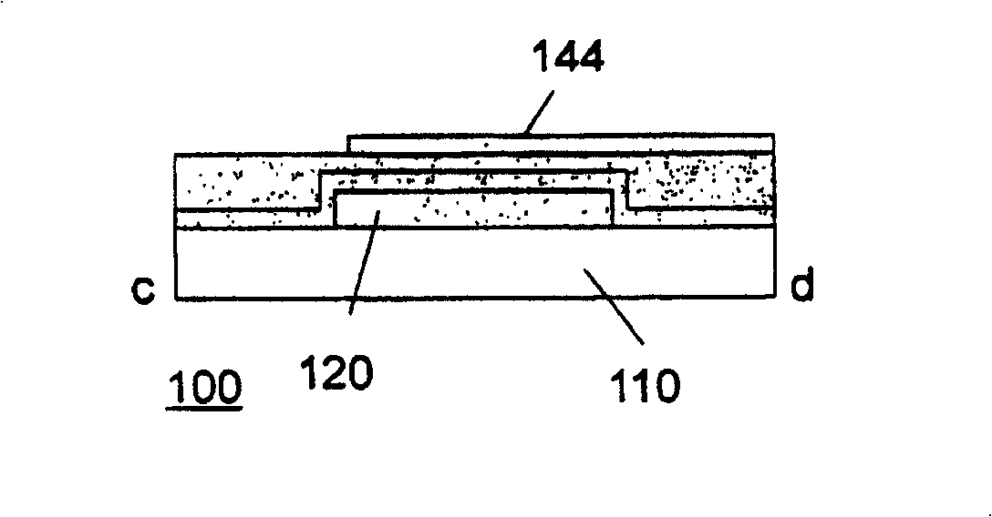
[0068] Figure 3A shows a top view of the active element array substrate according to the first embodiment of the present invention, and Figure 3B , Figure 3C , Figure 3D Draw separately Figure 3A Sectional view along section line a-b, section line c-d, section line e-f. Please also refer to Figure 3A to Figure 3D The active element array substrate 300 includes a substrate 310 , a plurality of scanning wires 320 , a plurality of data wires 330 , and a plurality of pixel units 340 . Wherein, a plurality of scan lines 320 , a plurality of data lines 330 and a plurality of pixel units 340 are all disposed on the substrate 310 .
[0069] For example, the substrate 310 can be a glass substrate, a quartz substrate or other transparent substrates. The scanning wires 320 can be aluminum alloy wires or wires formed of other suitable conductive materials, and the data wires 330 can be wires formed of chromium metal wires, aluminum alloy wires or other suitable conductive mate...
no. 2 example
[0077] Figure 4AIt shows the top view of the active element array substrate according to the second embodiment of the present invention, which is Figure 3A Deformation of the active element array substrate shown, and Figure 4B , Figure 4C , Figure 4D Draw separately Figure 4A Sectional view along section line a-b, section line c-d, section line e-f. Please also refer to Figure 4A to Figure 4D , the active element array substrate 400 of this embodiment is similar to the active element array substrate 300 of the first embodiment, but the main difference between the two is: in the active element array substrate 400 of this embodiment, the second drain 410 is located In the adjacent pixel unit 340 , it extends from above the scan line 320 to one side of the scan line 320 to below the adjacent pixel electrode 344 .
[0078] Please continue to refer Figure 4A to Figure 4D , when the first thin film transistor T1 of the adjacent pixel unit 340 ( Figure 4A When the fi...
no. 3 example
[0081] Figure 5A It shows the top view of the active element array substrate according to the third embodiment of the present invention, which is Figure 3A Deformation of the active element array substrate shown, and Figure 5B , Figure 5C , Figure 5D Draw separately Figure 5A Sectional view along section line a-b, section line c-d, section line e-f. Please also refer to Figure 5A to Figure 5D , the active element array substrate 500 of this embodiment is similar to the active element array substrate 300 of the first embodiment, but the main difference between the two is: in the active element array substrate 500 of this embodiment, only the odd or even The second thin film transistor T2 is only formed at the intersection of the data scanning wiring 330 and the scanning wiring 320 , so the left and right adjacent pixel units 340 have a shared second thin film transistor T2 . In addition, the second thin film transistor T2 of this embodiment has two second drains 51...
PUM
 Abstract
Description
Claims
Application Information