Method for gluing and chip loading on lead frame of integrated circuit or discrete device

A lead frame and discrete device technology is applied in the field of electronic component packaging and chip mounting technology to achieve the effects of improving utilization, reducing development costs, and large area

Active Publication Date: 2009-01-14
长电科技管理有限公司
View PDF5 Cites 0 Cited by
  • Summary
  • Abstract
  • Description
  • Claims
  • Application Information

AI Technical Summary

Problems solved by technology

[0013] The object of the present invention is to overcome above-mentioned deficiency, provide a kind of method for coating and mounting chip on the lead frame of novel integrated circuit or discrete device, this method can make coating thickness uniform, without bubble and coating unevenness phenomenon, when loading chip No chip shift or rotation issues

Method used


Image

  • Method for gluing and chip loading on lead frame of integrated circuit or discrete device
  • Method for gluing and chip loading on lead frame of integrated circuit or discrete device
  • Method for gluing and chip loading on lead frame of integrated circuit or discrete device

Examples


Embodiment 1

[0042] Embodiment 1 is the method for gluing on the lead frame of integrated circuit or discrete device, and the method comprises the following process steps:

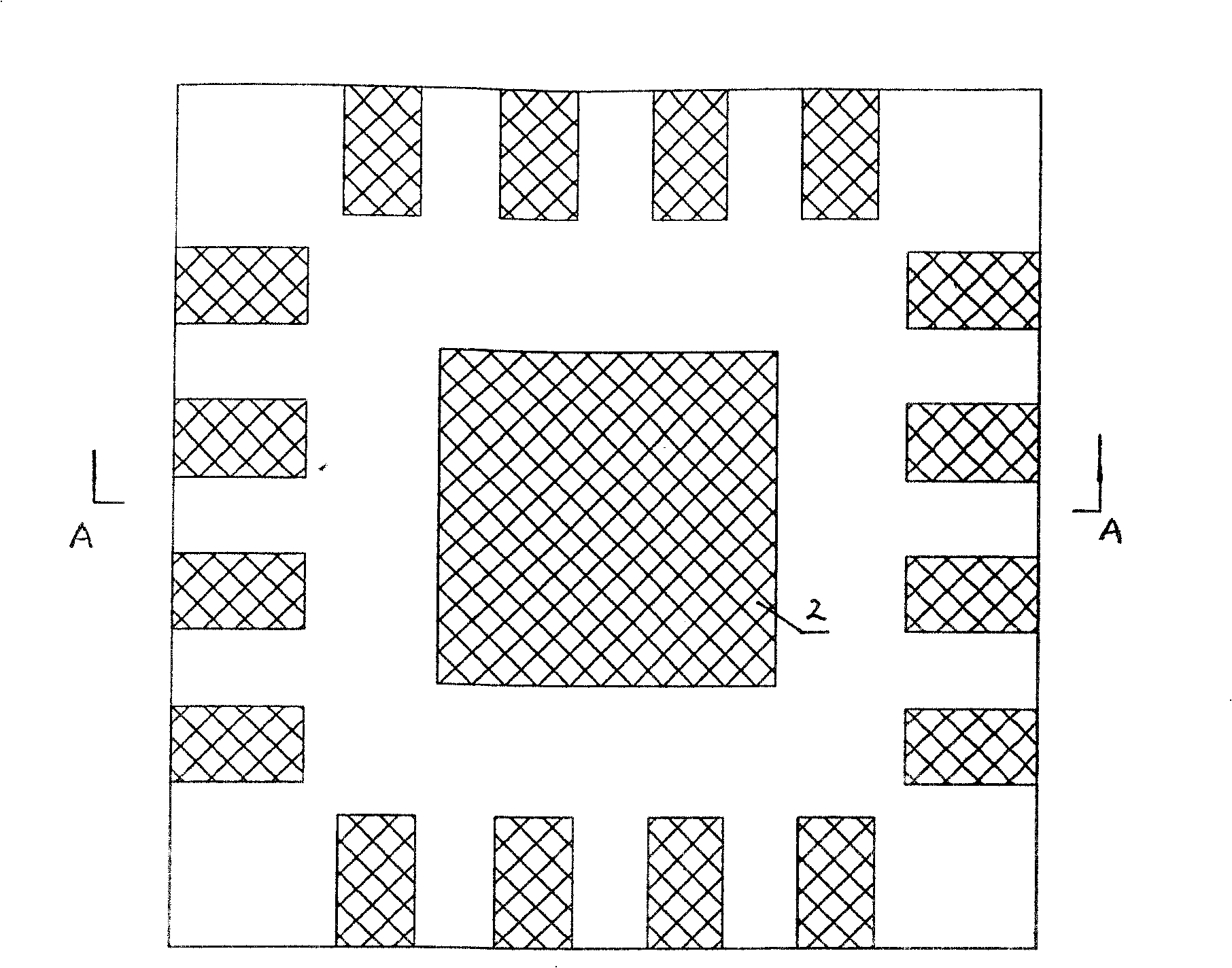
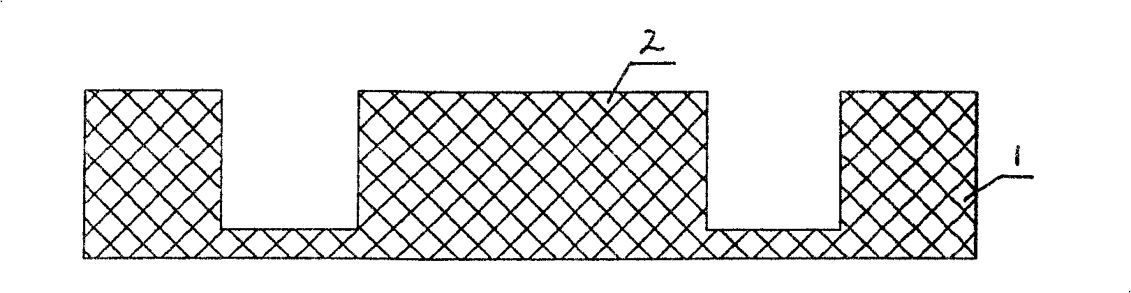
[0043] 1) Take the lead frame - take a piece of lead frame 1, such as figure 1 , 2 ;

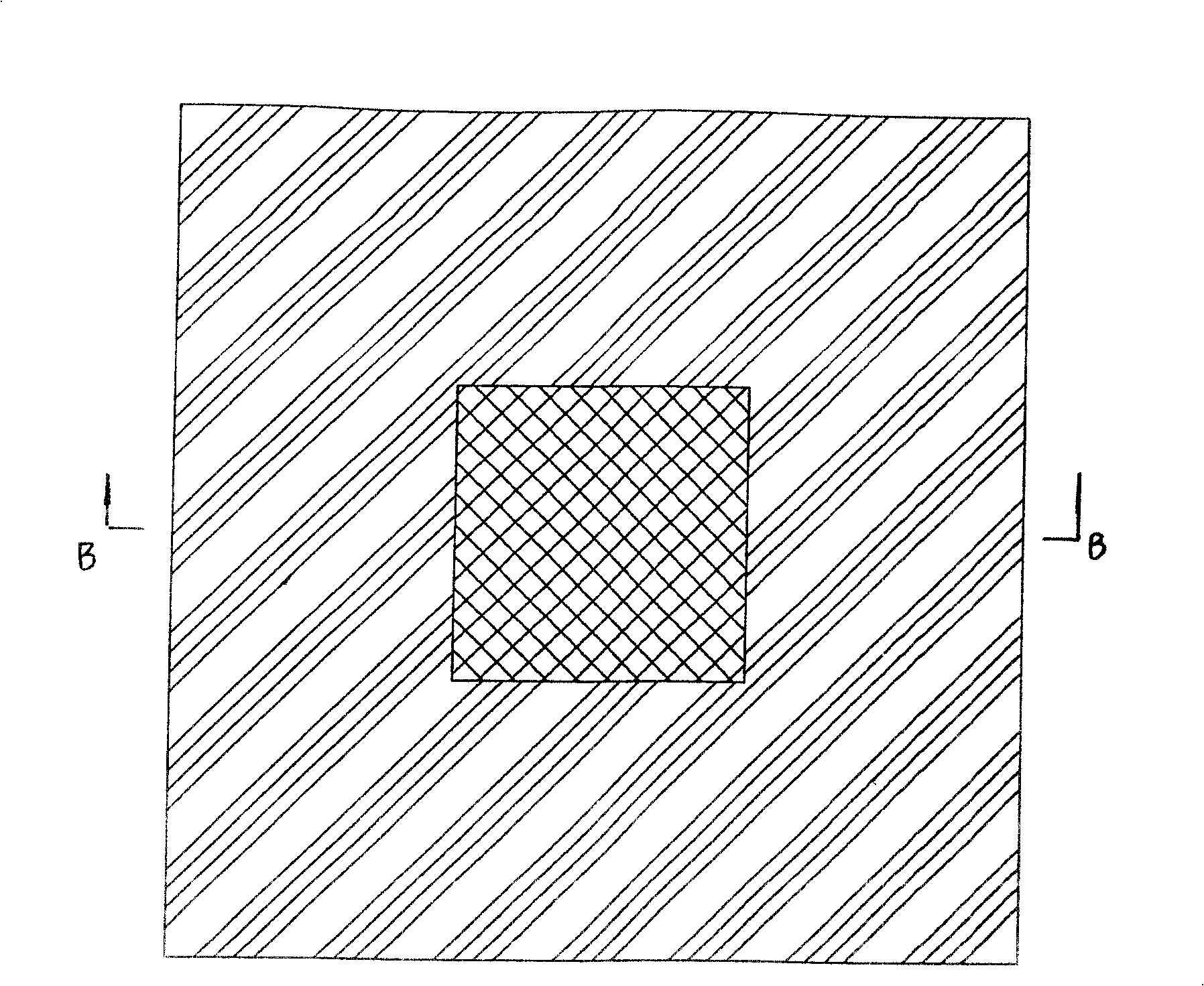
[0044] 2) Attaching the mask—cover the area of ​​the lead frame 1 that does not need to be loaded with the mask 3, and leave the area 4 on the base island 2 that needs to be loaded, such as image 3 , 4 ;

[0045] 3) Glue coating operation—use the glue coating method to apply glue 5 to the area 4 on the vacated base island of the lead frame 1 that needs to be loaded, such as Figure 5 , 6 ;

[0046] 4) Removing the mask - Remove the mask 3 covering the lead frame, such as Figure 7 , 8 ;

[0047] 5) Baking operation—baking the semi-finished lead frame that has been coated with glue 5 on the base island 4 for the first time;

[0048] 6) Softening glue operation - before loading, heat the semi-finished lead frame that has bee...

Embodiment 2

[0052] In the above steps, after the mask is removed in step 4, step 5 and step 6 can be skipped and chip loading 6 can be directly performed on it, and then baked and strengthened.

[0053] In each of the above embodiments, the chip loading, wherein the chip installed may refer to a chip chip, and may also be a chip resistor, a chip capacitor, a chip inductor, etc.; the chip mounting on the base island is not limited to Since it is only installed on the base island, it can also be mounted on the front or back of the lead frame other than the base island.


PUM


Abstract

A method for gluing and chip loading on lead frame includes providing a lead frame and using mask to cover region not to be loaded with chip as well as voiding out region to be loaded with chip, coating glue on region to be loaded with chips, removing off said mask, carrying out the first baking on lead wire frame with coated glue, heating and softening baked lead wire frame then placing chips on glue, carrying out the second baking on lead frame with loaded chips for making said frame and glue as well as chips to be firmly bound with each other.

Description

technical field [0001] The invention relates to a method for coating and mounting chips on an integrated circuit or discrete device lead frame. The invention belongs to the technical field of packaging chip packaging technology of electronic components. Background technique [0002] Traditionally, there are two methods of coating and mounting chips on the lead frame of integrated circuits or discrete devices: one is the method of dispensing glue on the lead frame, and the other is the method of coating and mounting chips on the back of the wafer. They have the following deficiencies respectively: [0003] 1. The method of dispensing glue on the lead frame [0004] 1. The thickness and shape of dispensing are not easy to control; [0005] 2. The extrusion hollow tube (apparatus) used for dispensing is easy to block, especially when multi-tube extrusion is required to install large chips, it is easier to increase the probability of blockage; [0006] 3. After the chip is l...

Claims


Application Information

Patent Timeline
Patent Type & Authority Patents(China)
IPC IPC(8): H01L21/50H01L21/58
CPCH01L24/27H01L24/83H01L2224/32245H01L2224/83192H01L2924/14H01L2924/00
Inventor 梁志忠王新潮于燮康谢洁人
Owner 长电科技管理有限公司
Why Eureka
Try Eureka