Semiconductor anti-static protection structure

A protection structure and anti-static technology, applied in the direction of semiconductor devices, semiconductor/solid-state device components, circuits, etc., can solve the problems of high breakdown voltage and damage, and achieve the effect of reducing the turn-on voltage and making it easier to turn on.

Active Publication Date: 2009-04-01
SHANGHAI HUAHONG GRACE SEMICON MFG CORP
View PDF1 Cites 0 Cited by
  • Summary
  • Abstract
  • Description
  • Claims
  • Application Information

AI Technical Summary

Problems solved by technology

When ESD occurs, the discharged electrostatic charge will cause two parasitic transistors of the protection device, namely figure 2 The PNP tube and NPN tube in the conduction, such as image 3 As shown, the device will produce the phenomenon of Snapback (step recovery)
However, due to the breakdown of the reverse PN junction of the N well due to the opening of these two parasitic transistors, its breakdown voltage is as high as 30-50V. With such a high breakdown voltage, the internal circuit to be protected may be earlier than its When turned on, it will be destroyed by ESD electrostatic charge

Method used


Image

  • Semiconductor anti-static protection structure
  • Semiconductor anti-static protection structure
  • Semiconductor anti-static protection structure

Examples


Embodiment Construction

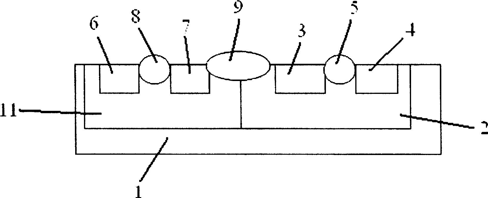
[0014] The semiconductor anti-static protection structure of the present invention can be found in Figure 4 As shown, a P-type substrate 1 is included, and an N-well implantation region 2 and a P-well implantation region 11 are included on the P-type substrate 1; a P-type implantation region 3 is included in the N-well implantation region 2 and an N-type implantation region 4, separated by an oxide layer isolation region 5 between the P-type implantation region 3 and the N-type implantation region 4 in the N-well implantation region 2; the P-well implantation region 11 also includes There is a P-type implanted region 6 and an N-type implanted region 7, and the P-type implanted region 11 of the P-well implanted region 11 is separated by another oxide layer 8 isolation region between the P-type implanted region 6 and the N-type implanted region 7; The P-type implant region 3 in the well implant region 2 is separated from the N-type implant region 7 of the P well implant region ...


PUM


Abstract

The invention discloses an Anti-static protection structure for a semiconductor, and the structure comprises a P type substrate. The P type substrate comprises an N well injection region and a P well injection region, which comprise respectively a P type injection region and an N type injection region. The P type injection region and the N type injection region are separated by a separation region of oxide layer. The P type injection region in the N well injection region and the N type injection well in the P well injection region are separated by another separation region of oxide layer. A polysilicon is arranged on the separation region of oxide layer between the P type injection region in N well injection region and the N type injection region in the P well injection region. The invention effectively decreases the threshold voltage of the thyristor. On one hand, the process condition is not increased; on the other hand, the parasitic NPN pipe and the PNP pipe which are used for ESD discharge become easier to be opened. The invention gives full play to ESD capability.

Description

technical field [0001] The invention relates to a semiconductor device structure, in particular to a semiconductor antistatic protection structure. Background technique [0002] Today's popular process technology uses SCR (silicon controlled silicon structure) as an ESD (electrostatic discharge) protection device, such as figure 1 As shown, a P-type substrate 1 is included, and an N-well implantation region 2 and a P-well implantation region 11 are included on the P-type substrate 1; a P-type implantation region 3 is included in the N-well implantation region 2 and an N-type implantation region 4, separated by an oxide layer isolation region 5 between the P-type implantation region 3 and the N-type implantation region 4 in the N-well implantation region 2; the P-well implantation region 11 also includes There is a P-type implanted region 6 and an N-type implanted region 7, and the P-type implanted region 11 of the P-well implanted region 11 is separated by another oxide lay...

Claims


Application Information

Patent Timeline
Patent Type & Authority Patents(China)
IPC IPC(8): H01L27/04H01L23/60
Inventor 苏庆
Owner SHANGHAI HUAHONG GRACE SEMICON MFG CORP
Why Eureka
Try Eureka