Unlock instant, AI-driven research and patent intelligence for your innovation.

Non-volatile memory device and manufacturing method thereof

A technology of non-volatile storage and manufacturing method, which is applied in the field of manufacturing of memory elements, and can solve the problems of high resistance value of bit lines, difficulty in scaling down the size of memory cells, etc.

Active Publication Date: 2009-04-22
MACRONIX INT CO LTD
View PDF5 Cites 0 Cited by
  • Summary
  • Abstract
  • Description
  • Claims
  • Application Information

AI Technical Summary

Problems solved by technology

[0007] This conventional manufacturing method results in high resistance of the bit line, in addition, it is difficult to shrink the size of the memory cell due to the short channel effect caused by the thermal budget when shrinking the size of the memory cell

Method used


Image

  • Non-volatile memory device and manufacturing method thereof
  • Non-volatile memory device and manufacturing method thereof
  • Non-volatile memory device and manufacturing method thereof

Examples


Embodiment Construction

[0018] Reference numerals will be described in detail in the embodiments according to the present invention, and examples will be shown in the drawings. Wherever possible, the same reference numerals will be used in the drawings to represent the same or similar elements.

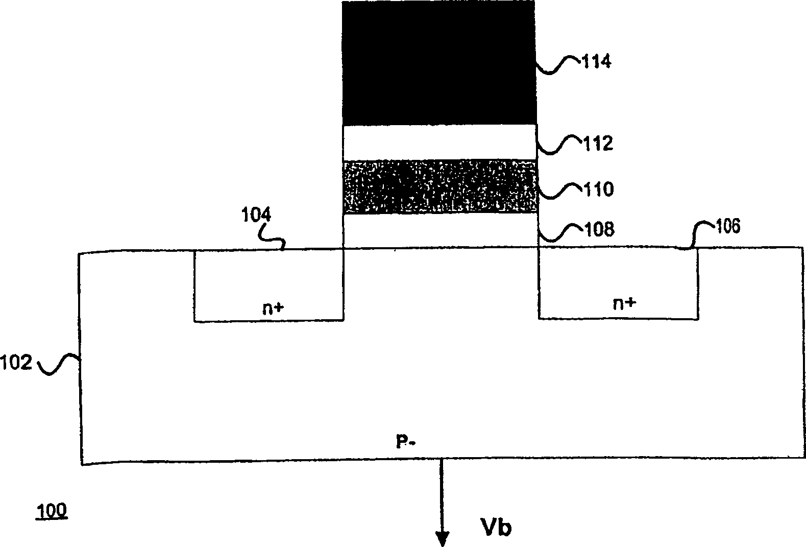
[0019] Figures 2A-2J An innovative method of fabricating a non-volatile memory element of the present invention is shown. Such as Figure 2A As shown in , the memory element 200 includes a charge trapping stack, which includes a first insulating layer 202 , a charge trapping layer 204 and a second insulating layer 206 formed on a semiconductor substrate 201 . The first and second insulating layers 202, 206 may be silicon oxide layers with a thickness of approximately 5 to 15 nanometers. The charge trapping layer 204 can be a silicon nitride layer with a thickness of about 2 to 8 nanometers. The charge trapping layer 204 can also be a high dielectric constant material layer, known as a high dielectric con...


PUM


Abstract

A method of manufacturing a non-volatile semiconductor memory device includes forming a sub-gate without an additional mask. A low word-line resistance is formed by a metal silicide layer on a main gate of the memory device. In operation, application of a voltage to the sub-gate forms a transient state inversion layer that serves as a bit-line, so that no implantation is required to form the bit-line.

Description

technical field [0001] The present invention relates to a manufacturing method of a memory element, and in particular to an innovative manufacturing method of a non-volatile memory element. Background technique [0002] Non-volatile memory elements are now widely used for data storage. Unlike traditional volatile storage devices, non-volatile storage devices can retain stored data even without power supply. For example: Read Only Memory (ROM), Programmable Read Only Memory (PROM), Erasable Programmable Read Only Memory (EPROM), Electrically Erasable Programmable Read Only Memory (EEPROM), and commonly known as Flash memory Flash erasable programmable read-only memory (flash EEPROM) is a kind of non-volatile storage elements. [0003] A memory element is typically composed of an array of memory cells. The advantage of the flash memory unit is that the data in a block can be erased at a time instead of one byte at a time like the traditional one. Each memory cell includes ...

Claims


Application Information

Patent Timeline
Patent Type & Authority Patents(China)
IPC IPC(8): H01L21/8247H01L21/336H01L27/115H01L29/788H10B69/00
CPCH01L27/115H01L27/11568H10B69/00H10B43/30
Inventor 何家骅施彦豪吕函庭赖二琨谢光宇
Owner MACRONIX INT CO LTD