
Coater/developer and coating/developing method

A development method and coating technology, which is applied in the direction of photography, photoplate making process coating equipment, instruments, etc., can solve the problems of affecting the refractive index of light, uneven line width accuracy, water non-permeation, etc., and achieve high uniformity in the plane , high precision effect

Inactive Publication Date: 2009-04-29
TOKYO ELECTRON LTD
View PDF7 Cites 0 Cited by
  • Summary
  • Abstract
  • Description
  • Claims
  • Application Information

AI Technical Summary

Problems solved by technology

In this case, there is a possibility that the eluted components adhere to the surface of the lens 10 and reduce the accuracy of the line width of the transferred circuit pattern.
In addition, even if the eluted component does not adhere to the surface of the lens 10, if the eluted component is contained in the water film, it will affect the refractive index of light, and there is a concern that the resolution will be reduced and the line width accuracy will be uneven in the plane.
In addition, resists for ArF are generally hydrophobic, but water is not completely impermeable, so there is the same problem as the above case

Method used

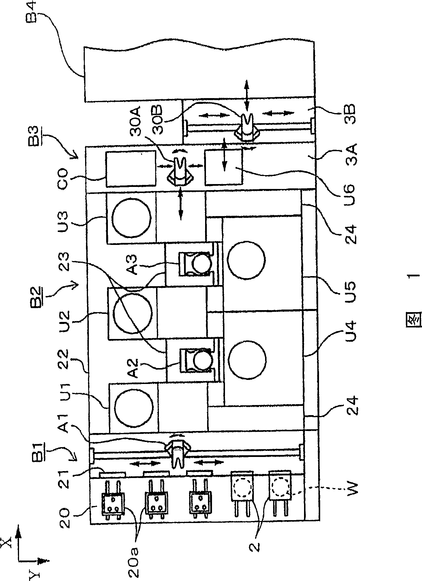
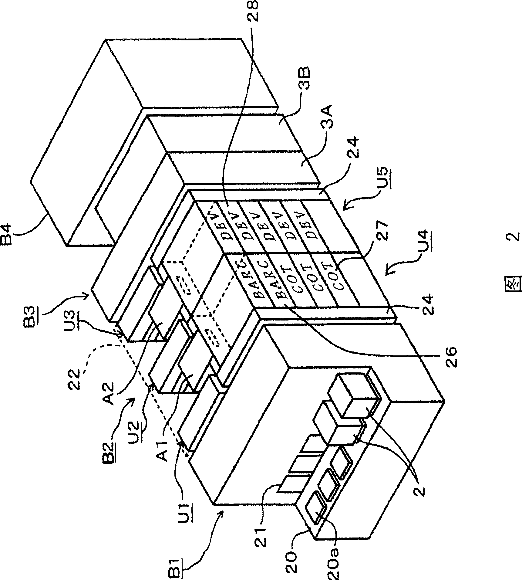
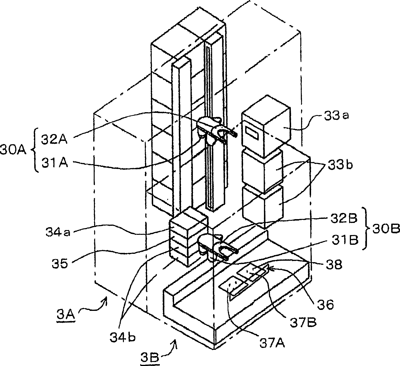

Image

  • Coater/developer and coating/developing method
  • Coater/developer and coating/developing method
  • Coater/developer and coating/developing method

Examples


Embodiment 1

[0076] This example is an example in which water washing treatment is performed before liquid immersion exposure. The wafer W was processed in the order of application of a methacrylic resist (resist A)→PAB treatment→water washing treatment (5 to 10 seconds)→exposure→PEB treatment→development. The line width of the resist pattern formed on the wafer W was measured using a length measuring SEM after development. The results are shown in FIG. 15 . In addition, in order to easily understand the effect of water washing when compared with the comparative example described later, the target value of the line width of the resist pattern was set to 90 nm. That is, resist A and resists B and C described below are all called methacrylic resists, and the main resin components are the same, but the acid generating components contained in the resists are respectively different. , is a resist whose main components are the same, but whose detailed components are different, and which have c...

Embodiment 2

[0078] This example is an example in which the same treatment as in Example 1 was performed except that a methacrylic resist (resist B) was applied instead of the resist A. exist Figure 16 The middle indicates the result of the measured line width.

Embodiment 3

[0080] This example is an example in which the same treatment as in Example 1 was performed except that a methacrylic resist (resist C) was applied instead of the resist A. exist Figure 17 The middle indicates the result of the measured line width.


PUM


Abstract

A coater / developer ensuring coating / development with high precision and high in-plane uniformity by suppressing the influence of components eluted from resist at the time of processing a substrate subjected to liquid immersion exposure. The surface of the substrate is coated with resist using a coating unit, the substrate is then cleaned using a first cleaning means such as a cleaning nozzle before exposed. Since the quantity of components eluted from the resist is small even if a liquid layer for passing light at the time of exposure is formed on the surface of the substrate, exposure can be carried out with high line width accuracy, and resultantly a resist pattern can be formed with high precision and high in-plane uniformity on the developed substrate.

Description

technical field [0001] The present invention relates to a coating and developing device and a coating and developing method. Background technique [0002] Conventionally, in the photoresist process, which is one of the semiconductor manufacturing processes, a resist is applied to the surface of a semiconductor wafer (hereinafter referred to as "wafer"), and the resist is exposed in a predetermined pattern. Thereafter, development is performed to form a resist pattern. Such processing is generally performed using a system in which an exposure device is connected to a coating / development device for coating and developing a resist. [0003] In addition, in recent years, device patterns tend to be more and more miniaturized and thinned, and there is a strong demand for higher exposure resolution. Therefore, development of exposure technology based on extreme ultraviolet light exposure (EUVL) (=Extreme Ultra Violet Lithography), electron beam projection exposure (EPL) (=Electro...

Claims


Application Information

Patent Timeline
Patent Type & Authority Patents(China)
IPC IPC(8): H01L21/027G03F7/38G03F7/16G03F7/20G03F7/30
CPCG03F7/70341G03F7/162H01L21/67028G03F7/2041G03F7/168H01L21/67051G03F7/3021G03F7/70925H01L21/02057
Inventor 山本太郎京田秀治
Owner TOKYO ELECTRON LTD
Learn More