
Semiconductor separation structure and its forming method

An isolation structure and semiconductor technology, applied in the fields of semiconductor devices, semiconductor/solid-state device manufacturing, electric solid-state devices, etc., can solve the problems of complex process and many processes, and achieve the effect of simple process, less process and low cost

Active Publication Date: 2009-06-10
SEMICON MFG INT (SHANGHAI) CORP +1
View PDF6 Cites 0 Cited by
  • Summary
  • Abstract
  • Description
  • Claims
  • Application Information

AI Technical Summary

Problems solved by technology

However, the above-mentioned method is complicated in technology and has many manufacturing processes, and it does not fundamentally solve the internal stress problem caused by the introduction of the nitrogen-containing lining layer; the process method of forming an oxide lining layer under the nitrogen-containing lining layer has more processes , and the stress problem between the nitrogen-containing liner and the oxide liner will also occur

Method used


Image

  • Semiconductor separation structure and its forming method
  • Semiconductor separation structure and its forming method
  • Semiconductor separation structure and its forming method

Examples


Embodiment Construction

[0035] The specific embodiments of the present invention will be described in detail below in conjunction with the accompanying drawings.

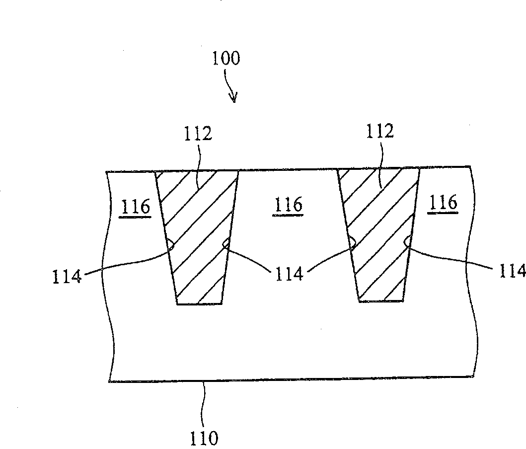
[0036] The semiconductor isolation structure formed by the method of forming the shallow trench isolation structure in the prior art will generate stress between the sidewall of the isolation trench and the semiconductor substrate. If the above stress cannot be eliminated, it will cause electrons in the semiconductor substrate or The electron mobility of holes changes, so that transistors with different channel lengths, especially transistors with short channel lengths, have different carrier mobility, which ultimately leads to instability in the performance of semiconductor devices.

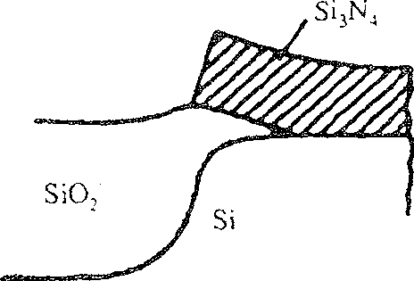
[0037] The prior art provides a variety of technical solutions for reducing the stress between the sidewall of the isolation trench and the semiconductor substrate. Most of them adopt the process of forming a nitride layer on the inner wall of the isolation t...


PUM


Abstract

A method for forming a semi-conductor isolation structure comprises the following steps: the underlayer of semi-conductor is provided; a multi-hole insulating layer is formed on the underlayer of semi-conductor; an insulating and obstructing layer is formed on the multi-hole insulating layer; photoresist mask film is formed on the insulating and obstructing layer; the photoresist mask film is made into a design, thus the underlayer of semi-conductor has an active area and an isolation area; the insulating and obstructing layer and the multi-hole insulating layer corresponding to the active area are corroded to form an isolating groove; the photoresist is removed; the isolating groove is filled with monocrystal line silicon; the monocrystal line silicon is made flat. The invention also provides a semi-conductor isolating structure, which consists of the underlayer of semi-conductor, isolating areas formed on the underlayer of semi-conductor and an active area positioned between the isolating areas. The isolating areas consist of a multi-hole insulating layer on the underlayer of semi-conductor and an insulating and obstructing layer on the multi-hole insulating layer. The semi-conductor isolating structure formed through the above method reduces efficiently the stress between the side walls of shallow isolating groove and a substrate.

Description

technical field [0001] The invention relates to the technical field of semiconductor manufacturing process, in particular to a semiconductor isolation structure and a forming method thereof. Background technique [0002] Semiconductor integrated circuits generally contain active regions and isolation regions between the active regions, which are formed prior to fabrication of the active devices. The methods for forming isolation regions in the prior art mainly include local oxidation isolation process (LOCOS) or shallow trench isolation process (STI). The LOCOS process is to deposit a layer of silicon nitride on the surface of the wafer, and then perform etching to oxidize and grow silicon oxide on part of the recessed area. Active devices are grown in areas defined by silicon nitride. However, there is a "bird's beak" phenomenon of silicon nitride edge growth in local oxidation isolation, such as figure 1 As shown, this is due to the difference in thermal expansion betwe...

Claims


Application Information

Patent Timeline
Patent Type & Authority Patents(China)
IPC IPC(8): H01L21/762H01L27/02
Inventor 叶好华毛刚
Owner SEMICON MFG INT (SHANGHAI) CORP
Learn More