Illuminating device

A technology for light-emitting devices and light-emitting bodies, applied in semiconductor devices, electrical components, circuits, etc., can solve the problems of high serial thermal resistance, thick product thickness, and inability to apply high-power light-emitting diode packaging, etc., to improve light-receiving efficiency and structure. thin effect

Active Publication Date: 2009-06-10
IND TECH RES INST
View PDF4 Cites 0 Cited by
  • Summary
  • Abstract
  • Description
  • Claims
  • Application Information

AI Technical Summary

Problems solved by technology

[0007] However, the above two packaging processes are prone to reliability problems due to the high thermal resistance in series. In addition, the products of this process use stacking technology, which causes the problem of excessive thickness of the product. When processing from the front, the depth of the groove must be Shallow designs (such as Figure 4A to Figure 4C ), for the convenience of processing, because of the shallow depth of the groove, the light-receiving effect is poor
[0008] another example Figure 5A to Figure 5C and Figure 6A to Figure 6C , which is a schematic diagram of the packaging process and assembly application of the ceramic substrate and the injection molded lead frame, wherein, if a ceramic material is used as the material of the substrate 50 (such as Figure 5A to Figure 5C ), it will cause the problem of high cost, and the aluminum substrate 51 must be used for assembly applications. In addition, for Figure 6A to Figure 6C , the use of injection molding will also cause the series thermal resistance to be too high, so it cannot be applied to the packaging of high-power light-emitting diodes, and it is also the same as the above ( Figure 4A to Figure 4C ), limited by the shallow depth of the groove, resulting in the problem of poor light collection effect

Method used


Image

  • Illuminating device
  • Illuminating device
  • Illuminating device

Examples


Embodiment

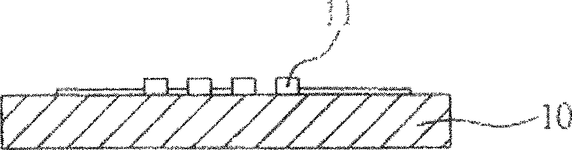
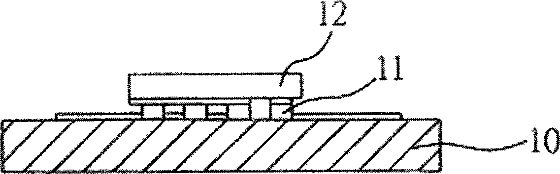
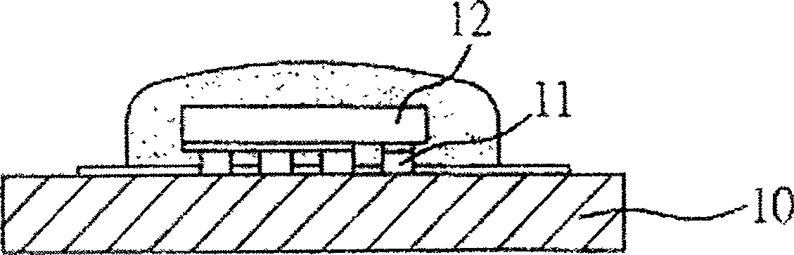
[0031] Such as Figure 7A to Figure 7E , Figure 8A to Figure 8B , Figure 9A to Figure 9B , Figure 10 , Figure 11 , Figure 12 , Figure 13 and Figure 14, which are related drawings of the light emitting device of the present invention. Wherein, it should be noted that the drawings are all simplified schematic diagrams, and only schematically illustrate the basic structure of the present invention. Therefore, only the components related to the present invention are shown in the accompanying drawings, and the displayed components are not drawn with the number, shape and size ratio of the actual implementation, and the number, shape and size ratio of the actual implementation are one An optional design, and its component layout shape may be more complex.

[0032] Such as Figure 7A to Figure 7E As shown, it is a schematic diagram of the structural combination of the light-emitting device of the present invention. After the light-emitting device of the present invention ...


PUM


Abstract

The invention is a light emitter to emit light after connected with power supply, at least comprising: luminous body having at least two electrodes to connect with power supply to make the luminous body offer a light source where the electrodes and the light outgoing surface of the luminous body are on the same side; bearing body with a groove to hold the luminous body, where the groove corresponds to the light outgoing surface and forms a diminishing shape close to the light outgoing and is equipped with connectors to connect with the light outgoing in the holding positions; and the invention has thin structure and makes the supply current path have advantages of low series thermal resistance and low cost, able to further increase light receiving efficiency by increasing groove depth.

Description

technical field [0001] The present invention relates to a light emitting device, in particular to a light emitting device applied to a high-power light emitting diode (LED). Background technique [0002] Light Emitting Diode (LED) is widely used in indicator lights, Advertising billboards, traffic lights, car lights, display panels, communication appliances, consumer electronics and other products. [0003] The flip-chip technology of light-emitting diodes is related to the industrial development of high-power light-emitting diodes in the future, and the packaging technologies used in today's industries are different. first as Figure 1A to Figure 1C As shown, it is a flip chip (flip chip) packaging process, such as Figure 1A , a plurality of electrically connected electrodes (bumps) 11 are formed on the aluminum substrate 10, as another example Figure 1B , the light-emitting diode chip 12 is bonded to the aluminum substrate 10 in a flip-chip manner, and then Figure 1...

Claims


Application Information

Patent Timeline
Patent Type & Authority Patents(China)
IPC IPC(8): H01L33/00H01L25/075H01L33/48H01L33/62
CPCH01L2224/83192H01L2224/16145H01L2224/32225H01L2224/48091H01L2224/48227H01L2224/73265H01L2924/00014H01L2924/00
Inventor 林明德林明耀郭家彰黄胜邦叶文勇
Owner IND TECH RES INST
Why Eureka
Try Eureka