Supercharge Your Innovation With Domain-Expert AI Agents!

Method for the manufacture of a non-volatile memory device and memory device thus obtained

An electrical device, access gate technology, applied in the field of non-volatile semiconductor memory, to achieve the effect of lack of mask alignment sensitivity

Inactive Publication Date: 2009-06-24
NXP BV
View PDF5 Cites 0 Cited by
  • Summary
  • Abstract
  • Description
  • Claims
  • Application Information

AI Technical Summary

Problems solved by technology

[0009] Another disadvantage of the method described above is that an additional masking step must be performed when different doping is required in the source and drain regions

Method used


Image

  • Method for the manufacture of a non-volatile memory device and memory device thus obtained
  • Method for the manufacture of a non-volatile memory device and memory device thus obtained
  • Method for the manufacture of a non-volatile memory device and memory device thus obtained

Examples


Embodiment Construction

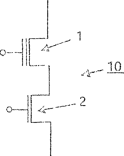
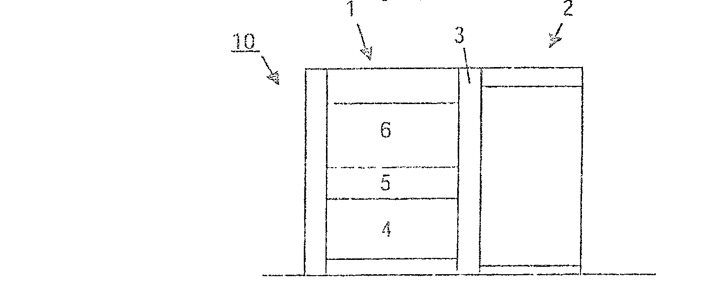
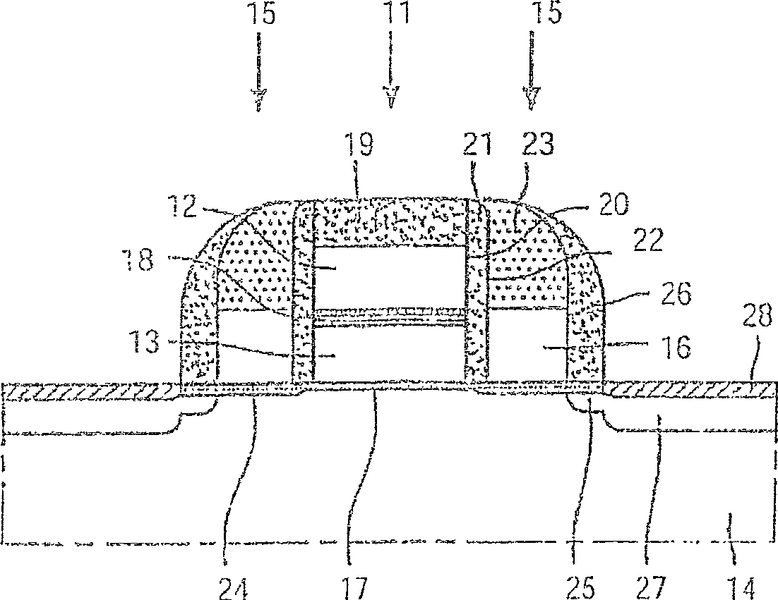
[0030] The present invention will be described below with respect to particular embodiments with reference to certain drawings but the invention is not limited thereto but only by the claims. The drawings described are only schematic and not restrictive. In the drawings, the size of some of the elements may be exaggerated and not drawn on scale for illustrative purposes. Although the term "comprising" is used in the present description and claims, it does not exclude other elements or steps. Although an indefinite or definite article is used when referring to a single noun, eg "a", this includes plural nouns unless specifically stated otherwise.

[0031] Furthermore, the terms first, second, third etc. in the description and claims are used to distinguish similar elements and are not necessarily used to describe a sequential or chronological order. It is to be understood that the terms so used are interchangeable under appropriate circumstances and that the embodiments of th...


PUM


Abstract

The invention relates to a method of processing a non-volatile memory cell (50) comprising a double gate stack and a single access gate. This approach combines treating the access gate with a drain implant separate from the source implant in a self-aligned manner. The method of the present invention does not require mask alignment sensitivity and enables self-aligned implantation of extended drains for erasing memory devices. Furthermore, the method provides a way to perform separate drain and source implants with different dopings without using additional masks.

Description

technical field [0001] The present invention relates to the field of non-volatile semiconductor memory. Background technique [0002] Non-volatile memory (NVM) is widely used in a variety of commercial and military electronics and equipment, such as cellular phones, radios, and digital cameras. The market for these electronic devices continues to demand devices with lower voltage, lower power consumption, and reduced chip size. [0003] The flash memory or flash memory cell includes a MOSFET with a floating gate between the control gate and the channel region. With the improvement of manufacturing technology, the size of the floating gate has been reduced to the order of nanometers. These devices are essentially miniature EEPROM cells in which electrons (or holes) are injected into nanofloating gates by tunneling through an oxide barrier layer. The charge stored in the floating gate changes the device threshold voltage. Stacked gate technology is employed in the fabricat...

Claims


Application Information

Patent Timeline
IPC IPC(8): H01L21/8247H01L29/423H01L21/8246
CPCH01L27/11521H01L29/42328H01L27/11568H10B43/30H10B41/30
Inventor 罗贝尔图斯·T·F·范斯海克
Owner NXP BV
Features
  • R&D
  • Intellectual Property
  • Life Sciences
  • Materials
  • Tech Scout
  • Unparalleled Data Quality
  • Higher Quality Content
  • 60% Fewer Hallucinations
Learn More