Supercharge Your Innovation With Domain-Expert AI Agents!

Integrated circuit memory and preparation method thereof

An integrated circuit and memory technology, applied in the field of integrated circuit memory and its preparation, can solve the problems of DRAM data access errors, increase coupling noise, affect component performance and reliability, etc., to improve device performance and reliability, and reduce coupling effect of effect

Active Publication Date: 2020-03-20
CHANGXIN MEMORY TECH INC
View PDF16 Cites 10 Cited by
  • Summary
  • Abstract
  • Description
  • Claims
  • Application Information

AI Technical Summary

Problems solved by technology

[0004] However, due to the continuous miniaturization of the size of semiconductor elements, the distance between the memory cells of the dynamic random access memory (DRAM) is also closer, which often leads to a very strong word line-word line coupling effect (word line-word line-coupling effect). word line coupling), that is, a serious coupling effect is likely to occur between two adjacent buried word lines 103 passing through each active region 102, which will increase coupling noise, affect device performance and reliability, and even cause DRAM data access error

Method used


Image

  • Integrated circuit memory and preparation method thereof
  • Integrated circuit memory and preparation method thereof
  • Integrated circuit memory and preparation method thereof

Examples


Embodiment Construction

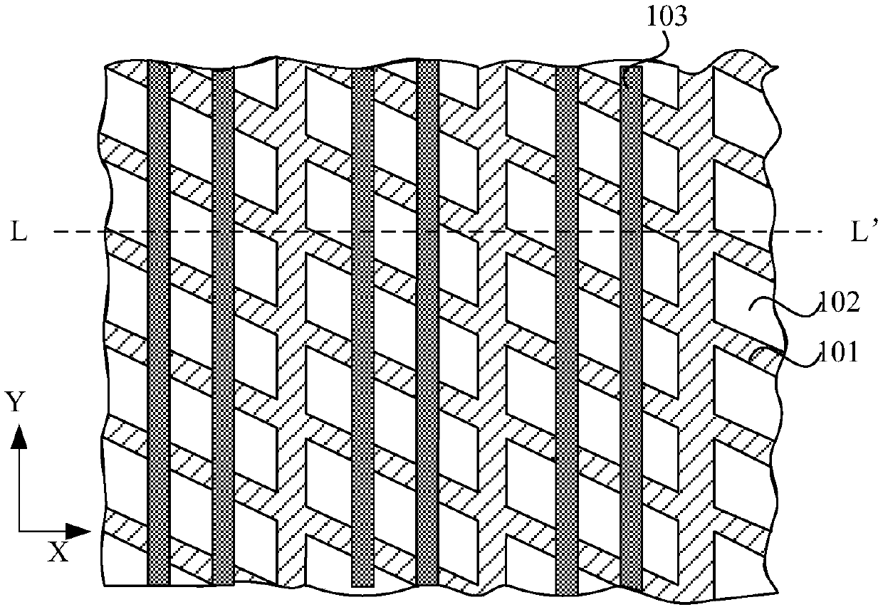
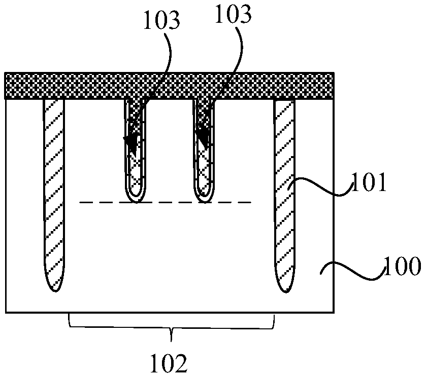
[0074] Continuing from the above, the electrical characteristics of a buried channel array transistor (BCAT) in a dynamic random access memory (DRAM) may vary depending on the depth from the upper surface of the semiconductor substrate to the bottom surface of its buried word line, for example, The magnitude of the coupling effect between two adjacent buried word lines in a dynamic random access memory (DRAM) can vary with the depth.

[0075] Based on this, the present invention provides an integrated circuit memory and a manufacturing method thereof, so that two adjacent buried word lines are arranged asymmetrically, and there is a certain height difference between the bottom surfaces of the two buried word lines The height difference is used to constrain and reduce the coupling effect between two adjacent buried word lines, thereby improving device performance and reliability.

[0076] The following is attached figure 2 , Figure 3A to Figure 3H The integrated circuit mem...


PUM

PropertyMeasurementUnit
sizeaaaaaaaaaa
sizeaaaaaaaaaa
thicknessaaaaaaaaaa

Abstract

The invention provides an integrated circuit memory and a preparation method thereof. According to the preparation method, an inclined ion implantation process with an inclined angle is adopted. Therefore, the two adjacent sacrificial structures have different etching selectivity due to different doping concentrations; mask openings with different depths are formed in the mask material layer; etching the semiconductor substrate by taking the mask material layer as a mask. According to the invention, the grooves with different depths can be obtained, and then the adjacent buried word lines withdifferent buried depths can be formed, so that the coupling effect between the adjacent buried word lines can be restrained and reduced through the height difference between the bottom surfaces of the adjacent buried word lines, and the efficiency and reliability of the device can be improved.

Description

technical field [0001] The invention relates to the technical field of integrated circuit manufacturing, in particular to an integrated circuit memory and a preparation method thereof. Background technique [0002] As a well-known semiconductor storage device, Dynamic Random Access Memory (Dynamic Random Access Memory, DRAM for short) is currently widely used in various electronic devices. Dynamic random access memory (DRAM) is composed of many repeated memory cells (cells), each memory cell is mainly composed of a transistor and a capacitor controlled by the transistor, and the memory cells are arranged in an array form, and each memory cell The cells are electrically connected to each other through a word line (WL for short) and a bit line (BL for short). In order to increase the density of dynamic random access memory (DRAM) to speed up the operation speed of components, and to meet the needs of consumers for miniaturized electronic devices, the recent design of the chan...

Claims


Application Information

Patent Timeline
Patent Type & Authority Applications(China)
IPC IPC(8): H01L27/108H10B12/00
CPCH10B12/34H10B12/37H10B12/038H10B12/053H10B12/488
Inventor 不公告发明人
Owner CHANGXIN MEMORY TECH INC
Features
  • R&D
  • Intellectual Property
  • Life Sciences
  • Materials
  • Tech Scout
  • Unparalleled Data Quality
  • Higher Quality Content
  • 60% Fewer Hallucinations
Learn More