Supercharge Your Innovation With Domain-Expert AI Agents!

A group III-V compound semiconductor and a method for producing the same

A compound and semiconductor technology, applied in the field of III-V compound semiconductors, can solve problems such as brightness drop

Inactive Publication Date: 2009-07-08
SUMITOMO CHEM CO LTD
View PDF3 Cites 0 Cited by
  • Summary
  • Abstract
  • Description
  • Claims
  • Application Information

AI Technical Summary

Problems solved by technology

[0008] In this method, during the growth of the p-GaN layer, the InGaN layer is cracked and indium metal or indium nitride crystals are precipitated, resulting in a significant decrease in brightness (Journal of Crystal Growth, 248, 498, 2003)

Method used


Image

  • A group III-V compound semiconductor and a method for producing the same

Examples


Embodiment 1

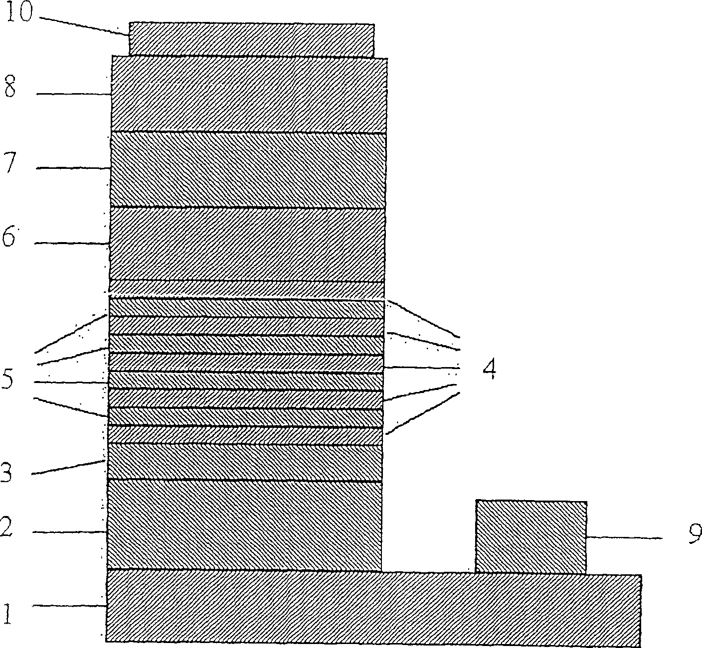
[0097] Supplying TMG and ammonia as raw materials and hydrogen as a carrier gas, a low-temperature grown GaN buffer layer was grown on the C-plane of sapphire at 490°C.

[0098] Once the supply of TMG was stopped, the temperature was raised to 1090°C, and then TMG, ammonia, and silane were supplied as raw materials and hydrogen as a carrier gas to grow an n-type GaN layer with a thickness of 3 μm, and then the supply of silane was stopped to grow a thickness of 300nm undoped GaN layer. After stopping the supply of TMG and silane and then cooling to 785°C, supplying TEG and ammonia as raw materials and nitrogen as a carrier gas, a GaN layer with a thickness of 100 nm was grown, and then the following procedure was repeated 5 times in which, at 50 kPa TEG, TMI, and ammonia as raw materials and nitrogen as a carrier gas were supplied under a pressure of 100 nm to grow an InGaN layer with a thickness of 3 nm and a GaN layer with a thickness of 15 nm. The details of the growth pro...

Embodiment 2

[0105] An LED was obtained by the same operation as in Example 1 except that the thickness of the p-type GaN layer was changed to 450 nm. LEDs were evaluated under the same conditions as in Example 1. The results are shown in Table 1.

Embodiment 3

[0107] An LED was obtained by the same operation as in Example 1 except that the thickness of the p-type GaN layer was changed to 300 nm. LEDs were evaluated under the same conditions as in Example 1. The results are shown in Table 1.


PUM


Abstract

The invention provides a III-V group compound semiconductor. The III-V group compound semiconductor comprises an n-type layer, a p-type layer represented by the formula InaGabAlcN having a thickness of not less than 300 nm, and a multi-quantum well structure existing between the n-type layer and the p-type layer, so The multiple quantum well structure has at least two quantum hydrazine structures including two barrier layers and a quantum well layer represented by InxGayAlzN between the barrier layers; and the R / α ratio is not more than 42.5%, where R is determined by X-ray diffraction The measured average mole fraction of indium nitride in the quantum well layer, α is the mole fraction of indium nitride calculated from the wavelength of light emitted from the III-V group compound semiconductor due to current injection.

Description

technical field [0001] The present invention relates to a III-V group compound semiconductor having the formula In a Ga b al c N(a+b+c=1, 0≤a<1, 0<b≤1, 0≤c<1) represents a p-type layer and a quantum layer comprising a barrier layer and a quantum well layer between the barrier layers well structure, the quantum well layer consists of the formula In x Ga y al z N (x+y+z=1, 0<x<1, 0<y<1, 0≤z<1) represents. Background technique [0002] Currently, using the formula In d Ga e al f N(d+e+f=1, 0≤d≤1, 0≤e≤1, 0≤f≤1) group III-V compound semiconductor as a light-emitting device emitting green, blue, purple or ultraviolet light . [0003] The application of white light-emitting light-emitting devices incorporating light-emitting materials and fluorescent materials to backlights or lighting has been studied. Since special crystals containing, for example, indium nitride can change the emission wavelength by changing the mole fraction of indium nitride ...

Claims


Application Information

Patent Timeline
Patent Type & Authority Patents(China)
IPC IPC(8): H01L33/00H01L33/06H01L33/32
CPCH01L33/32H01L33/06B82Y20/00H01L33/007
Inventor 佐佐木诚高田朋幸
Owner SUMITOMO CHEM CO LTD
Features
  • R&D
  • Intellectual Property
  • Life Sciences
  • Materials
  • Tech Scout
  • Unparalleled Data Quality
  • Higher Quality Content
  • 60% Fewer Hallucinations
Learn More