Metal connecting structure, semiconductor device and its manufacturing method

A technology of semiconductors and oxide semiconductors, which is applied in semiconductor/solid-state device manufacturing, semiconductor devices, semiconductor/solid-state device components, etc., can solve the problems of high resistance of tungsten connection holes and increase of tungsten connection holes, and reduce interconnection Resistor, reduced delay, and simplified manufacturing process

Active Publication Date: 2009-07-22
SEMICON MFG INT (SHANGHAI) CORP +1
View PDF5 Cites 0 Cited by
  • Summary
  • Abstract
  • Description
  • Claims
  • Application Information

AI Technical Summary

Problems solved by technology

However, as the feature size of the device continues to shrink, the resistance of the tungsten connection hole continues to increase, especially after the manufacturing process enters the 45nm technology node, the resistance of the tungsten connection hole itself has become unacceptably large

Method used


Image

  • Metal connecting structure, semiconductor device and its manufacturing method
  • Metal connecting structure, semiconductor device and its manufacturing method
  • Metal connecting structure, semiconductor device and its manufacturing method

Examples


Embodiment Construction

[0039] In order to make the above objects, features and advantages of the present invention more comprehensible, specific implementations of the present invention will be described in detail below in conjunction with the accompanying drawings.

[0040] In the following description, numerous specific details are set forth in order to provide a thorough understanding of the present invention. However, the present invention can be implemented in many ways other than those described here, and those skilled in the art can make similar extensions without departing from the connotation of the present invention. Accordingly, the invention is not limited to the specific implementations disclosed below.

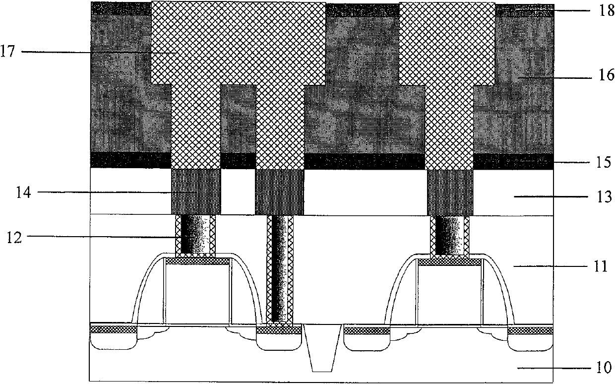
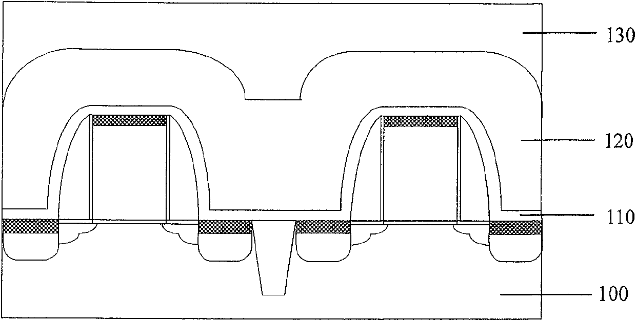
[0041] The manufacturing method of the metal connection structure of the semiconductor device of the present invention adopts the dual damascene process to etch through holes and trenches respectively in the PMD layer and the intermetal dielectric layer (IMD, just metal 1), and fills t...


PUM


Abstract

The invention discloses a manufacturing method of a metal connecting structure, which comprises that: a first medium layer is deposited on the surface of a semiconductor substrate; a second medium layer is deposited on the surface of the first medium layer; with the dual damascene technique, a copper dual-damascene connecting structure is formed between the first medium layer and the second medium layer. The method of the invention can reduce the resistance of the metal connecting structure.

Description

technical field [0001] The invention relates to the technical field of semiconductor manufacturing, in particular to a method for manufacturing a metal connection structure of a semiconductor device and a semiconductor device. Background technique [0002] Today's semiconductor manufacturing technology is developing rapidly, semiconductor devices have a deep submicron structure, and integrated circuits already contain a huge number of semiconductor devices. In such a large-scale integrated circuit, the high-reliability and high-density connection between devices must not only be performed in a single layer, but also between multiple layers. Therefore, multi-layer interconnection structures are usually used for semiconductor devices connect. [0003] figure 1 Simplified schematic diagrams for semiconductor devices and interconnect structures. Such as figure 1 As shown, before the interconnection layer is formed in the backend of line (BEOL), it is usually necessary to dep...

Claims


Application Information

Patent Timeline
Patent Type & Authority Patents(China)
IPC IPC(8): H01L21/768H01L23/522
Inventor 宁先捷
Owner SEMICON MFG INT (SHANGHAI) CORP
Why Eureka
Try Eureka