Inverted misarrangement type ballast structural panel display device and its production technique

A flat-panel display and manufacturing process technology, applied in the manufacture of discharge tubes/lamps, image/graphic display tubes, control electrodes, etc., can solve the problems of inability to ensure the cathode emission capability of carbon nanotubes and different field emission capabilities

CN100527332CInactive Publication Date: 2009-08-12ZHONGYUAN ENGINEERING COLLEGE
1 Cites 0 Cited by

Patent Information

Authority / Receiving Office
CN · China
Patent Type
Patents(China)
Current Assignee / Owner
Publication Date
2009-08-12
Estimated Expiration
Not applicable · inactive patent

Smart Images

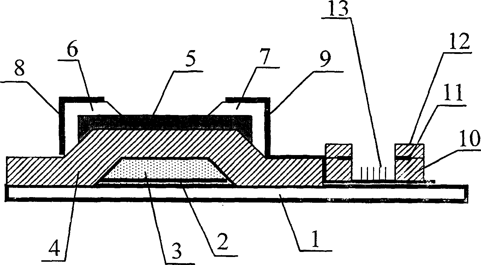
  • Figure 1
    Figure 1
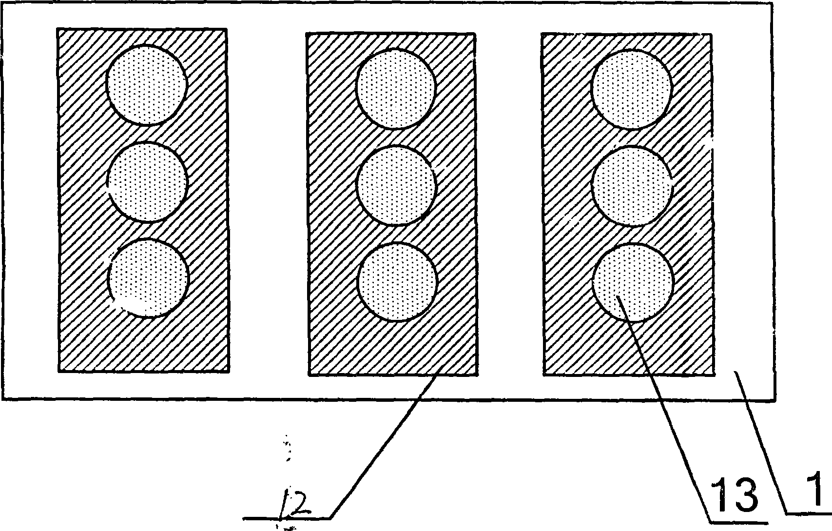
  • Figure 2
    Figure 2
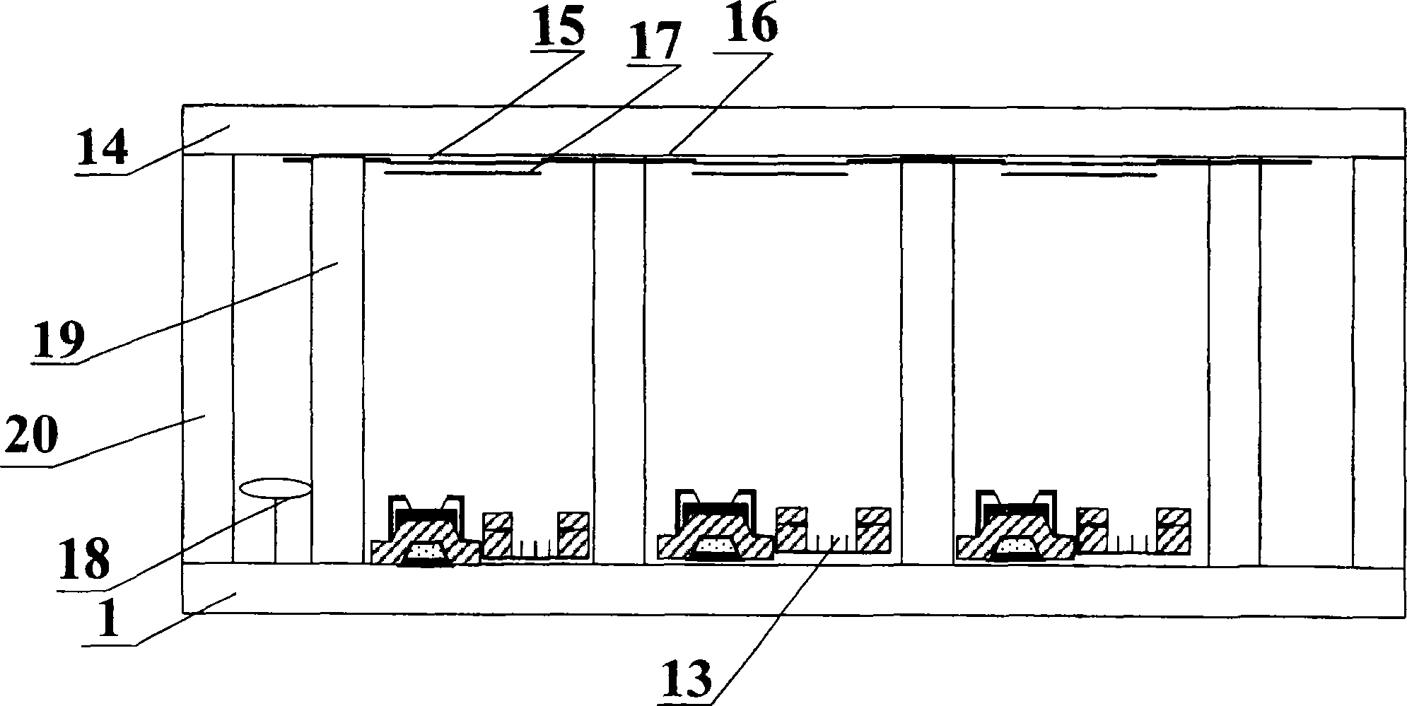
  • Figure 3
    Figure 3
Patent Text Reader

Abstract

The invention relates to a flat panel display with an inverted staggered ballast structure and its manufacturing process, comprising a sealed vacuum chamber composed of a cathode glass panel, an anode glass panel and surrounding glass frames; layer and the phosphor layer prepared on the anode conductive layer; the support wall structure and getter accessory components between the anode glass panel and the cathode glass panel, and the control grid, carbon nanotube cathode and inverted fault on the cathode glass panel Arrangement ballast structure; by adjusting the gate voltage, the current flowing through the carbon nanotube cathode can be further adjusted, thereby adjusting the ability of the carbon nanotube cathode to field-emit electrons, so that the overall carbon nanotube cathode can uniformly and stably emit a large number of electrons The effect of further improving the luminous uniformity of the whole device has the advantages of stable and reliable manufacturing process, simple manufacturing process, low manufacturing cost and simple structure.
Need to check novelty before this filing date? Find Prior Art

Description

technical field

[0001] The present invention belongs to the fields of plane display technology, electronic science and technology, vacuum science and technology, integrated circuit science and technology, and nano science and technology, and relates to device fabrication of flat panel field emission displays, in particular to It relates to the device manufacture of flat panel field emission display with carbon nanotube cathode, especially relates to a flat panel display with inverted staggered ballast structure and its manufacturing process. Background technique

[0002] Carbon nanotubes have a small tip curvature radius, high aspect ratio and good electrical conductivity. When an appropriate voltage is applied, a large number of electrons will be emitted, forming a unique cold field emission phenomenon, which has already attracted many researchers. of great importance. The field emission flat panel display made of carbon nanotubes as the cathode material is a new type of h...

Examples

Embodiment Construction

[0041] The present invention will be further described below in conjunction with the accompanying drawings and embodiments, but the present invention is not limited to these embodiments.

[0042] The flat panel display with an inverted staggered ballast structure includes a sealed vacuum chamber formed by a cathode glass panel 1, an anode glass panel 14 and surrounding glass frames 20; layer 15 and phosphor layer 17 prepared on the anode conductive layer; support wall structure 19 between the anode glass panel and the cathode glass panel and getter attachment 18. There are control grid 11, carbon nanotube cathode 13 and inverted staggered ballast structure on the cathode glass panel;

[0043] The inverted staggered ballast structure includes a cathode glass panel 1, a gate lead layer 2, a gate 3, a silicon dioxide insulating layer 4, an n-type doped silicon layer 5, a source 6, a drain 7, Source lead layer 8 , drain lead layer 9 , silicon dioxide isolation layer 10 , gate 11 ...