Semiconductor optoelectronic component and its cutting method

A technology of photoelectric components and cutting methods, which is applied in semiconductor devices, semiconductor/solid-state device manufacturing, photovoltaic power generation, etc., can solve problems affecting the light extraction effect of light-emitting diode crystal grains, and achieve improved light extraction efficiency, good appearance, and improved crystal grains. The effect of yield

Active Publication Date: 2009-08-12
EPISTAR CORP
View PDF5 Cites 0 Cited by
  • Summary
  • Abstract
  • Description
  • Claims
  • Application Information

AI Technical Summary

Problems solved by technology

However, because laser cutting will form a charred layer on the inner wall surface of the groove (90), it will form a charred area on the surface of the LED grain, which will affect the light extraction effect of the LED grain

Method used


Image

  • Semiconductor optoelectronic component and its cutting method
  • Semiconductor optoelectronic component and its cutting method
  • Semiconductor optoelectronic component and its cutting method

Examples


Embodiment Construction

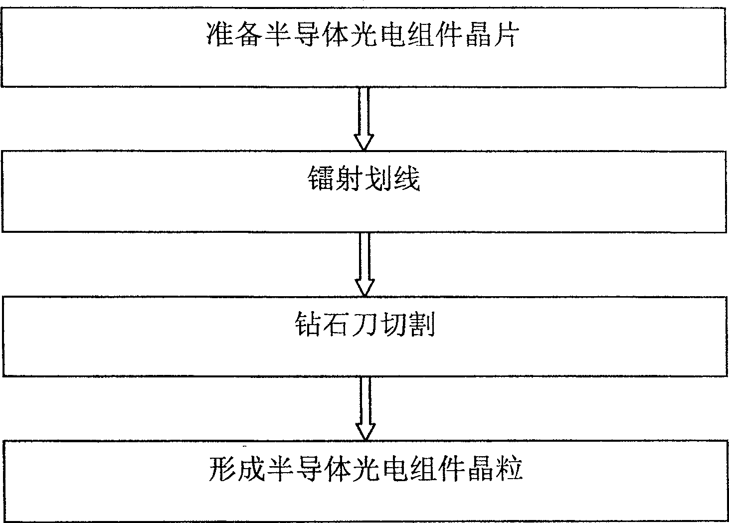
[0037] Please refer to figure 1 Shown, the cutting method of semiconductor optoelectronic component of the present invention is to comprise:

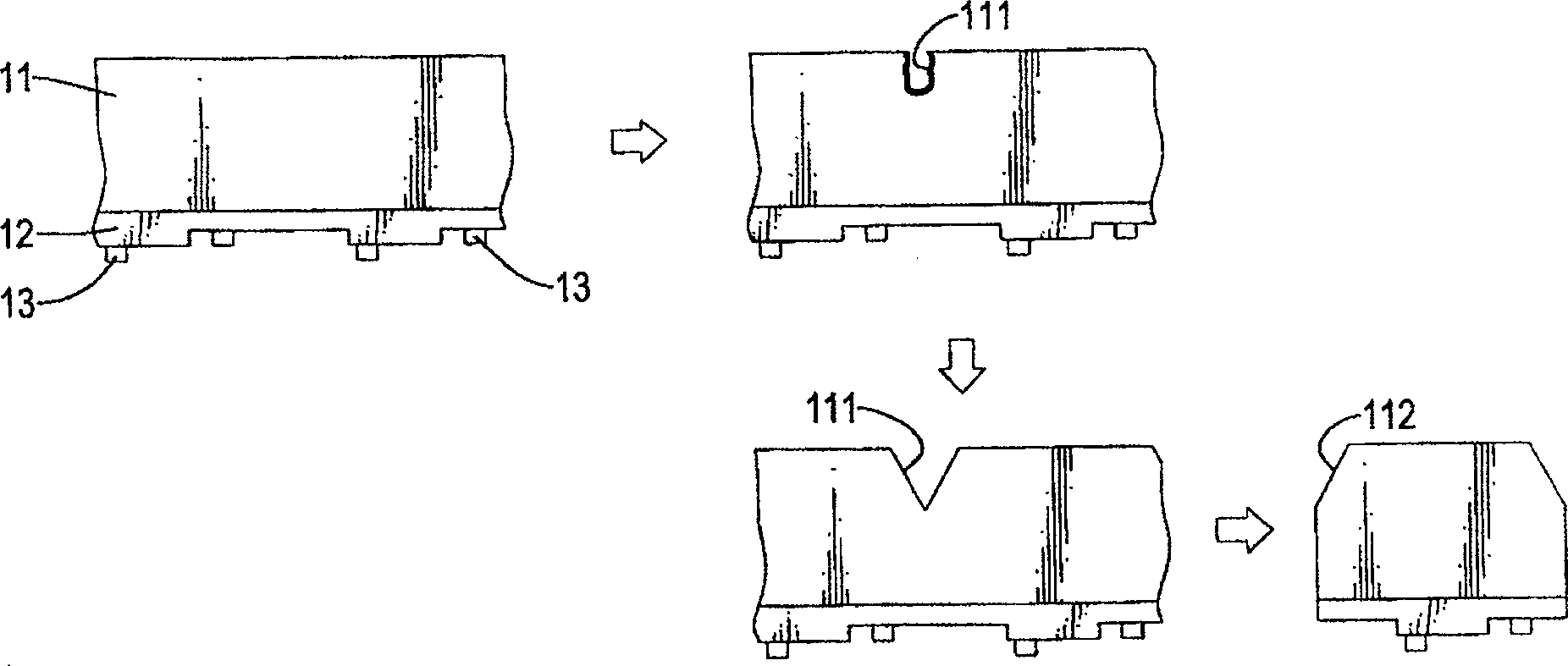
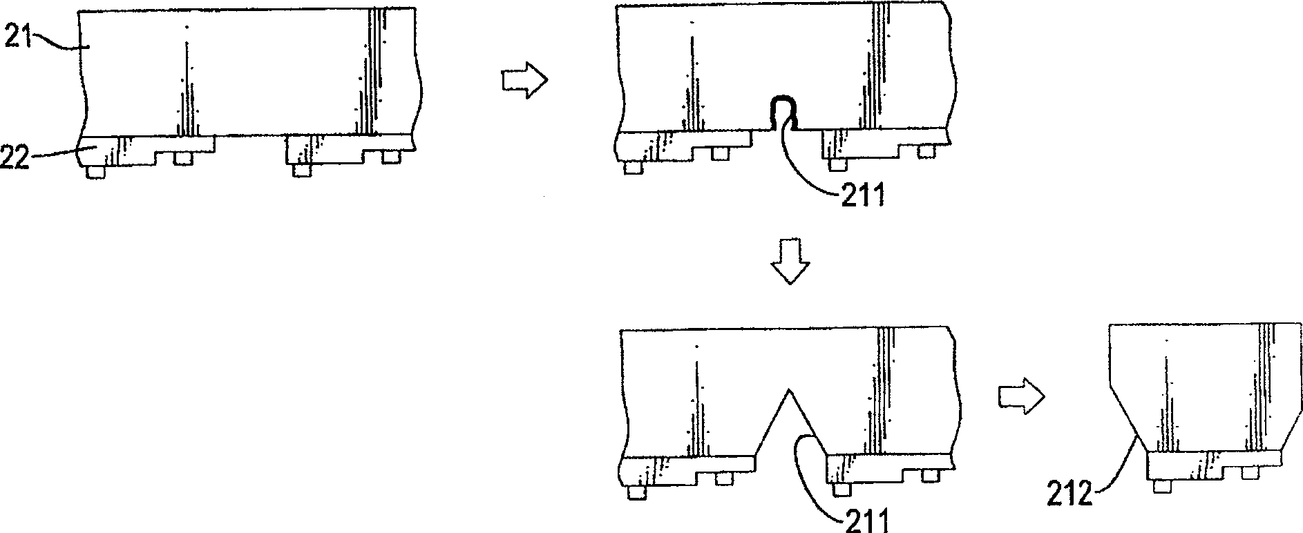
[0038] Prepare semiconductor optoelectronic component chips: please refer to figure 2 Shown, the semiconductor optoelectronic component chip is formed with an epitaxial silicon layer (12) on the substrate (11), and is provided with a metal electrode (13) on the epitaxial silicon layer (12), and this epitaxial silicon layer (12) material can be The semiconductor materials of III-V group compounds, such as materials such as GaN, GaS, GaP, InP, InGaAlN, InGaAlP, InGaAlAs and GaAlPAs; The epitaxial silicon layer (12) material can also be the semiconductor materials of II-VI group compounds, such as ZnO, Materials such as ZnSe, ZnS and ZnTe; the material of the epitaxial silicon layer (12) can also be semiconductor materials of group IV elements, such as Si and Ge and other materials.

[0039] Laser scribing: Use laser to draw a guide gr...


PUM


Abstract

A method for cutting a semi-conductor photoelectric assembly comprises the following steps of: preparation of a semi-conductor photoelectric assembly chip, wherein, the semi-conductor photoelectric assembly chip comprises a substrate and an epitaxial silicon layer formed on the surface of the substrate; laser marking, wherein, the laser is used to mark a guide groove on the surface of the semi-conductor photoelectric assembly chip; the cutting of a diamond cutter, wherein, the diamond cutter is used to cut in the groove; formation of semi-conductor photoelectric assembly grains are obtained, wherein, the semi-conductor photoelectric assembly chip is split along the marked groove to form the semi-conductor photoelectric assembly grains. The semi-conductor photoelectric assembly of the invention is provided with one substrate and one epitaxial silicon layer, the epitaxial silicon layer is formed on one surface of the substrate, one side of the substrate is provided with a rough surface, the rough surface is formed by the cutting of the diamond cutter in the guide groove which is produced by laser marking on the surface of the semi-conductor photoelectric assembly chip.

Description

technical field [0001] The invention relates to a semiconductor optoelectronic component and its cutting method, especially to a cutting method of a semiconductor optoelectronic component combined with electric jet cutting and diamond knife cutting, which can remove the scorched area on the crystal grain of the semiconductor optoelectronic component and reduce the diamond Knife loss. Background technique [0002] Since red, blue and green are the three primary colors of full-color, the application of high-brightness blue light-emitting diodes (LEDs) for full-color displays has been increasingly valued, and optical information access technology will also use short-wavelength blue light-emitting diodes as light sources. In addition, white light-emitting diodes derived from blue light-emitting diodes are also considered to be the next generation of lighting technology. [0003] Generally, the traditional cutting methods of light-emitting diodes include diamond knife cutting an...

Claims


Application Information

Patent Timeline
Patent Type & Authority Patents(China)
IPC IPC(8): H01L31/18H01L31/0236H01L21/78H01L21/304H01L21/301
CPCY02E10/50Y02P70/50
Inventor 程志青蔡棋
Owner EPISTAR CORP
Why Eureka
Try Eureka