Complementary type metal oxide semiconductor image sensor and manufacturing method therefor

An oxide semiconductor and image sensor technology, applied in semiconductor/solid-state device manufacturing, radiation control devices, electrical components, etc., can solve problems such as affecting image quality, increasing noise, and reducing component performance, reducing performance and avoiding dark current, the effect of reducing leakage current problems

Inactive Publication Date: 2009-09-02
UNITED MICROELECTRONICS CORP
View PDF4 Cites 0 Cited by
  • Summary
  • Abstract
  • Description
  • Claims
  • Application Information

AI Technical Summary

Problems solved by technology

The above-mentioned leakage current problem will cause the CMOS image sensor to generate a considerable dark current (dark current), which will increase the readout noise and affect the image quality, thereby reducing the performance of the device

Method used


Image

  • Complementary type metal oxide semiconductor image sensor and manufacturing method therefor
  • Complementary type metal oxide semiconductor image sensor and manufacturing method therefor
  • Complementary type metal oxide semiconductor image sensor and manufacturing method therefor

Examples


Embodiment Construction

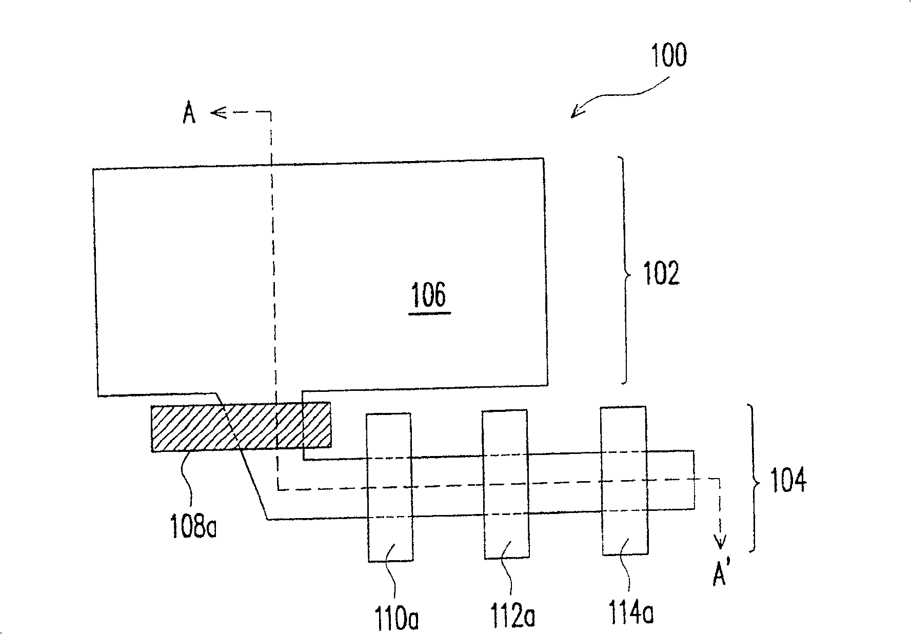
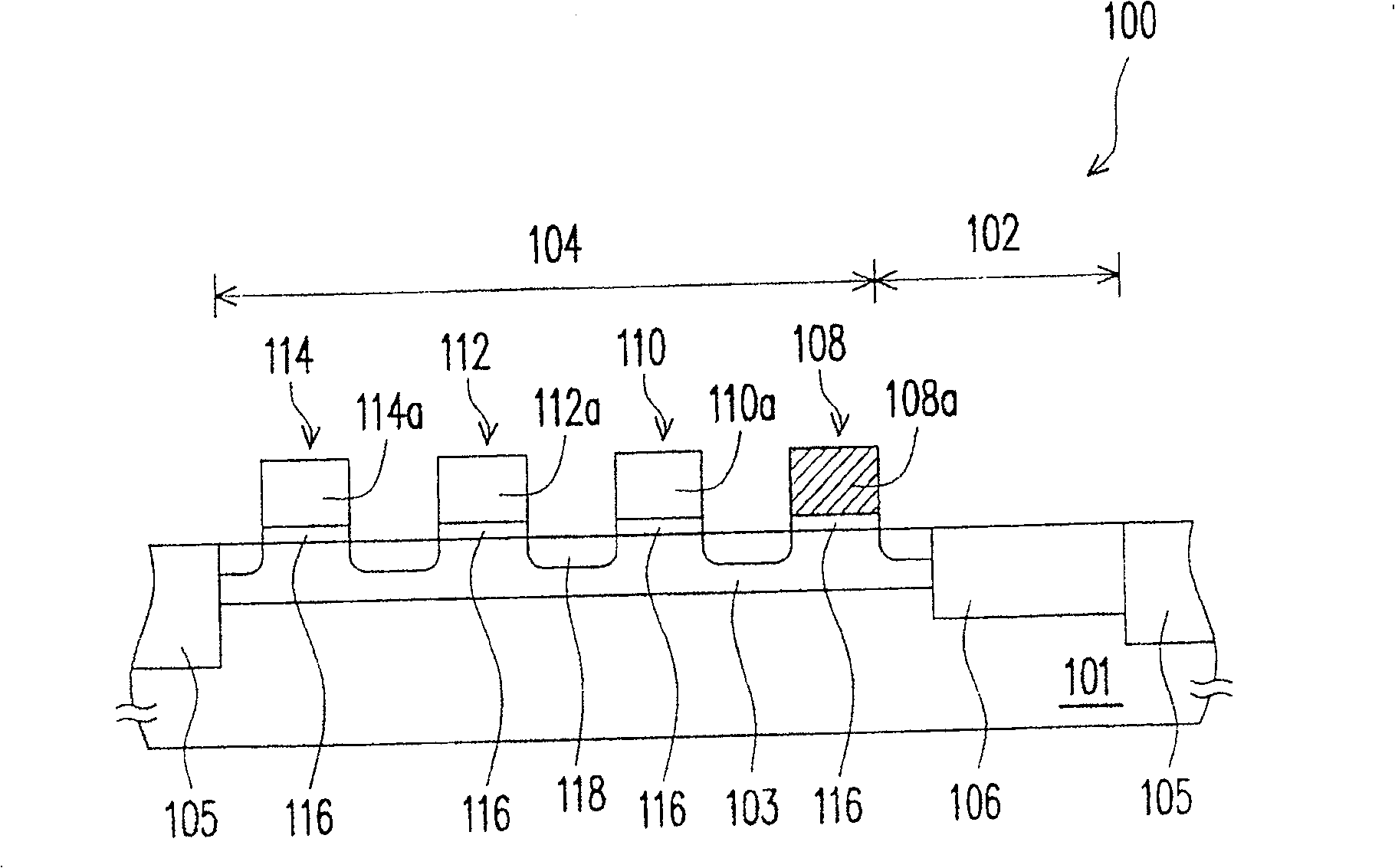
[0054] The present invention is applicable to CMOS image sensors with 3-T architecture or 4-T architecture, but is not limited thereto, and the present invention is also applicable to other CMOS image sensors with multiple transistor structures Image Sensor.

[0055] figure 1 It is a schematic top view of a CMOS image sensor according to an embodiment of the present invention. figure 2 shown as figure 1 Schematic cross-section along section line AA'.

[0056] Please also refer to figure 1 and figure 2 A CMOS image sensor 100 with a 4-T structure is composed of a substrate 101 , a photodiode 106 , a p-type gate structure 108 and a plurality of n-type gate structures 110 , 112 , 114 . Wherein, the substrate 101 is, for example, a silicon substrate or other semiconductor substrates. An isolation structure 105 is provided in the substrate 101 to define the photo-sensing region 102 and the transistor element region 104 . The isolation structure 105 is, for example, a shallo...


PUM


Abstract

A complementary metal oxide semiconductor image sensor includes a substrate, a photodiode, a p-type gate structure and a plurality of n-type gate structures. Wherein, the base has a light sensing area and a transistor element area. The photodiode is configured in the base of the light sensing area. The p-type gate structure is configured on the base of the transistor element region. A plurality of n-type gate structures are disposed on the base of the transistor element region.

Description

technical field [0001] The invention relates to an image sensor and a manufacturing method thereof, in particular to a complementary metal oxide semiconductor image sensor and a manufacturing method thereof. Background technique [0002] Complementary metal oxide semiconductor image sensor (CMOS image sensor, CIS) is compatible with complementary metal oxide semiconductor technology, so it is easy to integrate with other peripheral circuits on the same chip, and can greatly reduce the cost and consumption of the image sensor power. In recent years, CMOS image sensors have become a substitute for charge-coupled devices in low-cost applications, and the importance of CMOS image sensors is increasing day by day. [0003] The CMOS image sensor is composed of a photodiode and a plurality of transistors, wherein the photodiode is composed of a p-n junction formed by an n-type doped region and a p-type substrate, and the transistor is an n-type junction of an n-type gate. type tr...

Claims


Application Information

Patent Timeline
Patent Type & Authority Patents(China)
IPC IPC(8): H01L21/8238H01L27/146
Inventor 施俊吉
Owner UNITED MICROELECTRONICS CORP
Why Eureka
Try Eureka