Method for producing display substrate

A technology of substrate and light-transmitting area, which is applied in semiconductor/solid-state device manufacturing, static indicator, photolithography process of pattern surface, etc., can solve the problems of high process complexity and high cost

Inactive Publication Date: 2009-09-23
AU OPTRONICS CORP
View PDF5 Cites 2 Cited by
  • Summary
  • Abstract
  • Description
  • Claims
  • Application Information

AI Technical Summary

Problems solved by technology

[0009] However, although transflective panels have better display characteristics and wider application levels, the complexity and cost of the process are relatively high

Method used


Image

  • Method for producing display substrate
  • Method for producing display substrate
  • Method for producing display substrate

Examples


Embodiment Construction

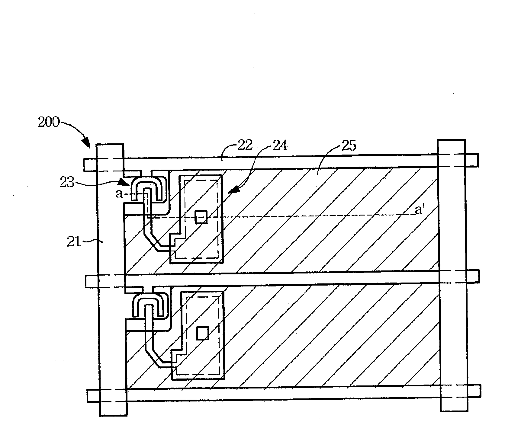
[0054] Please refer to figure 2, which is a top view of the display substrate of the present invention. Each pixel 200 of the display substrate at least includes a gate line 21 , a common line 22 , a TFT 23 , a capacitor structure 24 and a pixel electrode 25 . And technical content of the present invention, roughly with figure 2 The cross-sectional view of the a-a' line in the middle is introduced as follows.

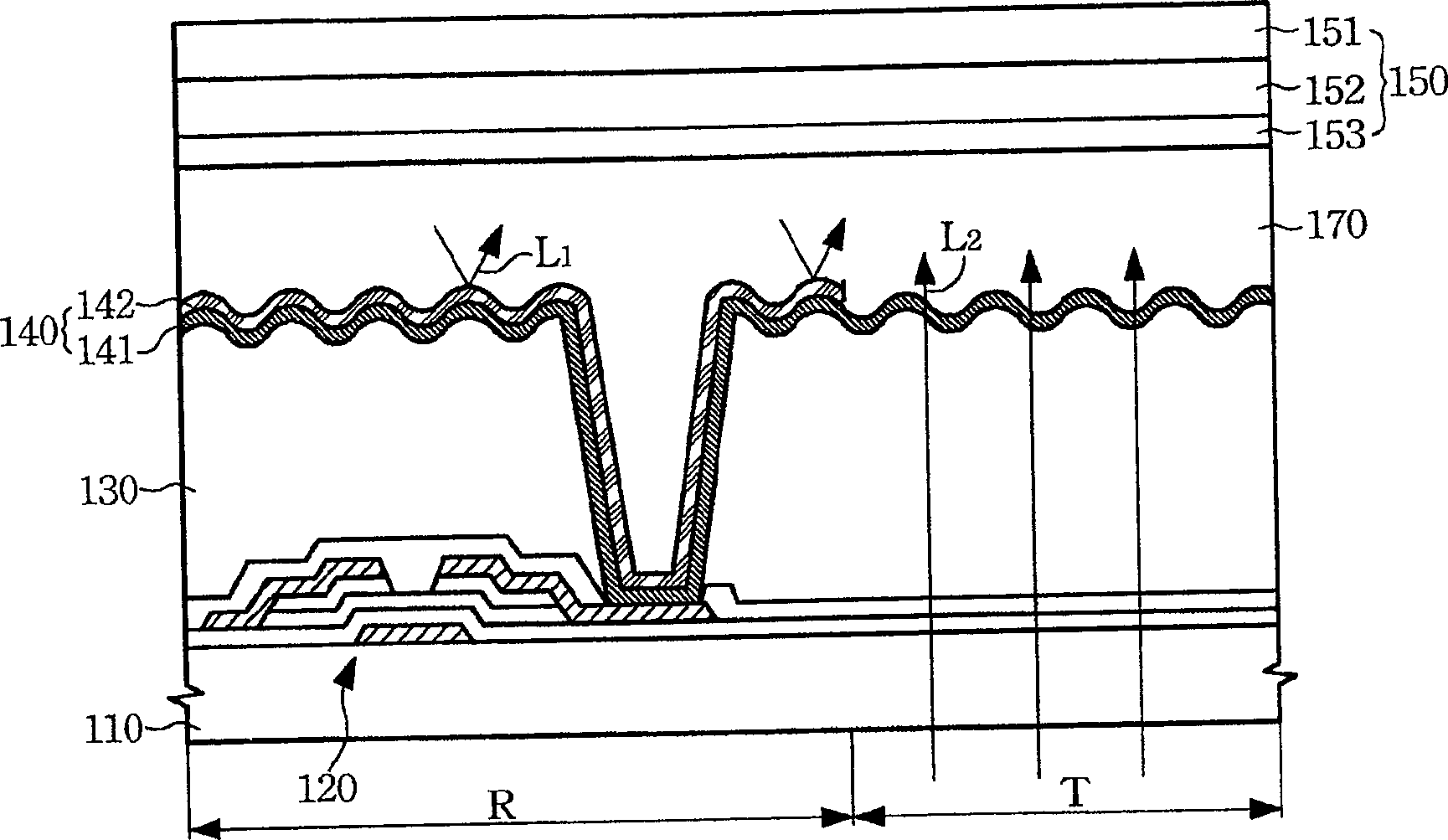
[0055] Please refer to Figure 3A to Figure 7B , which is a cross-sectional view of a display substrate in various structural forms of the present invention. Since the main technical content of the present invention lies in the display substrate in the transflective panel, and the color filter substrate disposed on the opposite side of the display substrate is similar to the known technology, so it will not be described in detail.

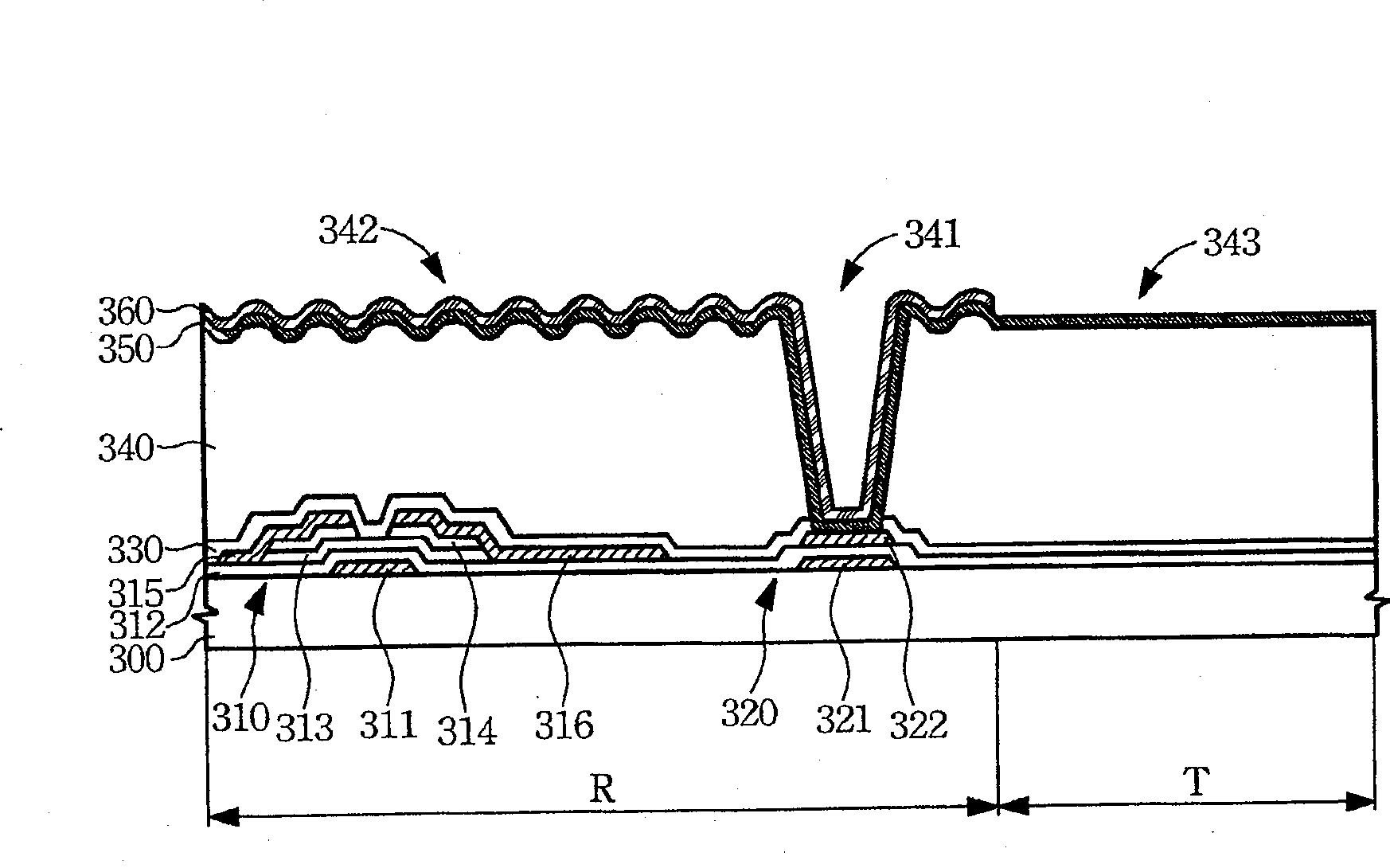
[0056] Please refer to Figure 3A , which is a structural form of the display substrate of the present invention. As shown in the f...


PUM

PropertyMeasurementUnit
transmittivityaaaaaaaaaa

Abstract

A method for manufacturing a display substrate. The method is applied to manufacture a transflective liquid crystal display. The method steps at least include: forming an active element and a capacitance structure on the substrate. A planarization layer is formed above the active components and capacitor structures. The planar layer is subjected to a photolithographic etching process using a mask with various light-transmitting regions, so as to simultaneously form different structural features on the planar layer.

Description

technical field [0001] The invention relates to a method for manufacturing a liquid crystal display panel, in particular to a method for manufacturing a transflective display substrate. Background technique [0002] Current liquid crystal displays (hereinafter referred to as LCDs) can be mainly divided into three categories: transmissive LCDs, reflective LCDs, and transflective LCDs. The transmissive LCD requires a backlight module as a backlight, which can have good visibility in a dark environment, but has the problems of excessive power consumption and too strong ambient light (such as sunlight). The reflective LCD replaces the transparent electrode layer with a reflective electrode layer, and uses external light as a light source without a backlight module. Therefore, the reflective LCD has the advantage of low power consumption, but it cannot work in a dark environment. [0003] The transflective LCD has a transmissive area and a reflective area at the same time, and ...

Claims


Application Information

Patent Timeline
Patent Type & Authority Patents(China)
IPC IPC(8): G02F1/1362G02F1/1333G02F1/133G03F1/00H01L21/00G03F1/28
Inventor 董畯豪黄国有黄宝玉
Owner AU OPTRONICS CORP
Why Eureka
Try Eureka