Optical system of focusing and leveling sensor

A technology of focusing and leveling device and optical system, applied in optics, photolithography process exposure device, microlithography exposure equipment, etc., can solve the problems of signal processing application, poor stability, error, etc. Small system measurement error, the effect of eliminating measurement error problem

Active Publication Date: 2009-11-11
SHANGHAI MICRO ELECTRONICS EQUIP (GRP) CO LTD
View PDF4 Cites 4 Cited by
  • Summary
  • Abstract
  • Description
  • Claims
  • Application Information

AI Technical Summary

Problems solved by technology

[0004] The above-mentioned first photoelectric measurement method is a differential measurement system with high stability, but because its optical system cannot eliminate the chromatic aberration of broadband light well, and the images of its various light spots are not all consistent with the projection objective lens The best focal plane coincides, so its optical system has a large system error, which puts a relatively large pressure on the subsequent signal processing
The latter two photoelectric measurement methods, in addition to having similar problems, are also less stable because they are not differential measurement systems, and because they only measure the absolute position of the silicon wafer, rather than measuring the relative position with respect to the projection objective. Therefore, this type of measurement method cannot compensate for the measurement error of the focusing and leveling sensor caused by the position drift of the projection objective lens.

Method used


Image

  • Optical system of focusing and leveling sensor
  • Optical system of focusing and leveling sensor
  • Optical system of focusing and leveling sensor

Examples


Embodiment Construction

[0027] Further illustrate the present invention below in conjunction with accompanying drawing.

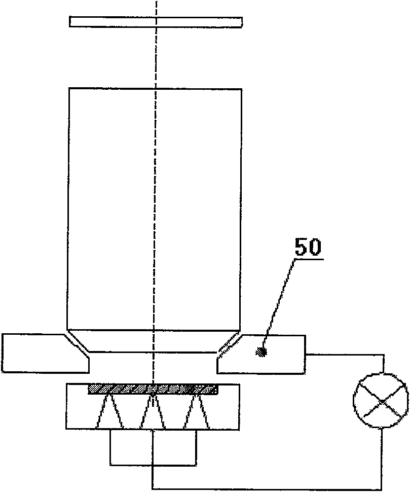
[0028] Such as figure 1 As shown, it is a schematic diagram of a simple structure of a photolithography machine, and the position marked 50 in the figure is a focusing and leveling sensor device. The optical system of the focusing and leveling device of the present invention includes a light source module, an illumination module, a projection imaging module, a detection imaging module and a detector module arranged sequentially along the propagation direction of the optical path;

[0029] Each component module of the optical system of the present invention will be described one by one below in conjunction with the accompanying drawings.

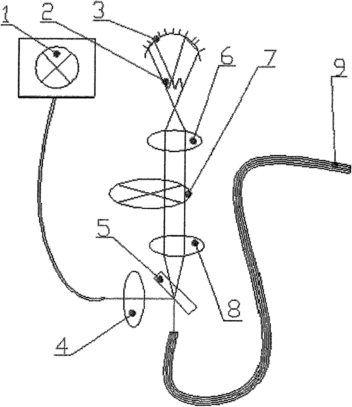
[0030] Such as figure 2 As shown, the light source module includes two alternately modulated narrowband optical modules, a broadband optical module, a coupling mirror 5 and a transmission cable 9; the narrowband optical module sequentially inc...


PUM


Abstract

The invention discloses an optical system of a focusing and leveling sensing device, which comprises a light source module, an illumination module, a projection imaging module, a detection imaging module and a detector module arranged in sequence along the propagation direction of an optical path. The invention adopts a reflective system, which eliminates the chromatic aberration effect of broadband light; adopts a unique stepped reflector to make the center of the image of each light spot on the upper surface of the silicon wafer at an ideal position, reducing the system measurement error , improving the measurement accuracy.

Description

technical field [0001] The present invention relates to the field of optical device design, in particular to an optical system of a focusing and leveling sensor device. Background technique [0002] The lithography machine is an exposure device that transfers the pattern on the mask to the object to be processed (such as silicon wafer, etc.) in a certain proportion, such as figure 1 shown. In this exposure device, it is necessary to keep the corresponding surface of the object to be exposed (assumed to be the upper surface) within the focal depth range of the projection objective lens in the exposure device; this requires a measurement system to measure the silicon wafer (here Generally refers to the relative position of the upper surface of the processed object (the same below) relative to the best focal plane of the projection objective. This measurement system is called a focus leveling sensor. With the sharp increase in the integration of integrated circuits, the line...

Claims


Application Information

Patent Timeline
Patent Type & Authority Patents(China)
IPC IPC(8): G03F7/20G03F9/00H01L21/00
Inventor 关俊李小平李志丹田湍金小兵
Owner SHANGHAI MICRO ELECTRONICS EQUIP (GRP) CO LTD
Why Eureka
Try Eureka