
Integrated semiconductor product comprising a metal-insulator-metal capacitor

一种金属电容器、半导体的技术,应用在电容器、半导体器件、固定电容器电介质等方向,能够解决表面积增加等问题

Inactive Publication Date: 2009-12-30
INFINEON TECH AG
View PDF4 Cites 0 Cited by
  • Summary
  • Abstract
  • Description
  • Claims
  • Application Information

AI Technical Summary

Problems solved by technology

And since the surface area specific capacitance value of a capacitor is determined by the thickness of the dielectric separation layer and the dielectric constant substantially, therefore, the surface area specific capacitance value of a capacitor can be obtained by using a capacitor having a high dielectric constant ( >8) to increase the dielectric, moreover, the insulating layer thinner than 60nm can also lead to an increase in surface area specific capacitance value

Method used


Image

  • Integrated semiconductor product comprising a metal-insulator-metal capacitor
  • Integrated semiconductor product comprising a metal-insulator-metal capacitor
  • Integrated semiconductor product comprising a metal-insulator-metal capacitor

Examples


Embodiment Construction

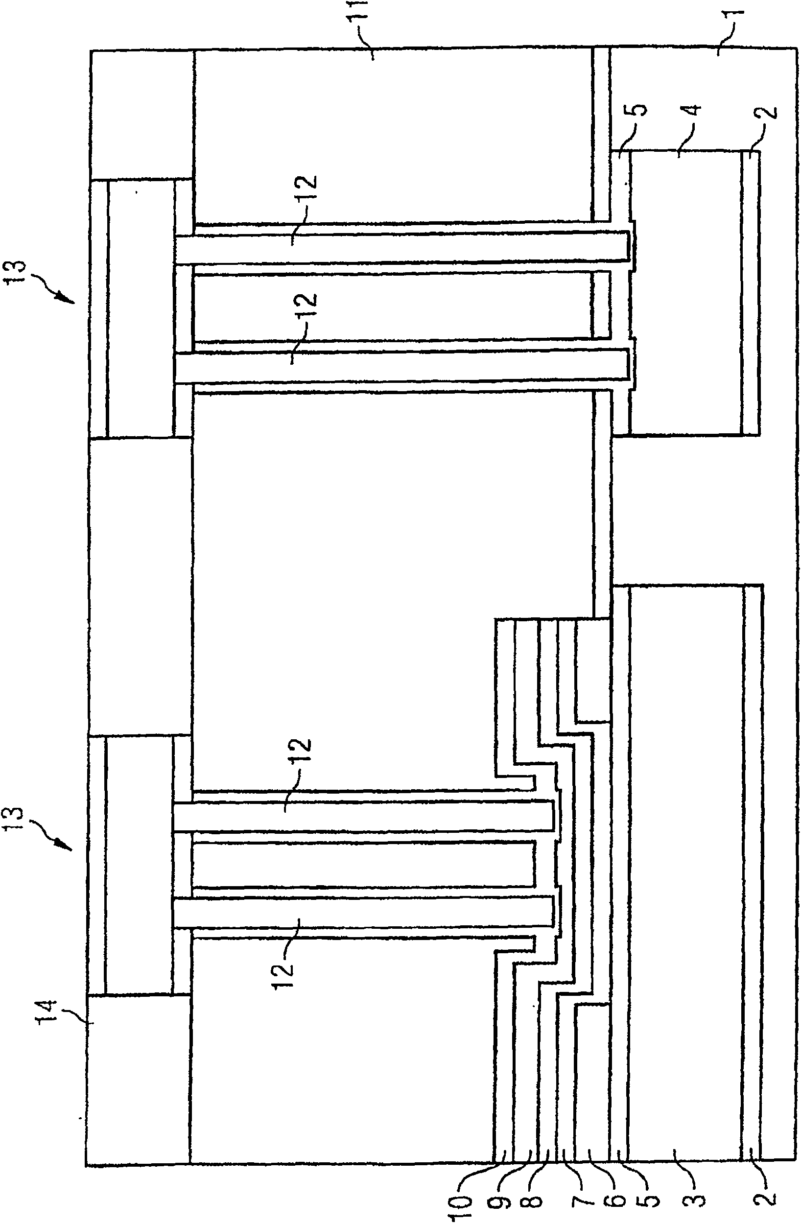
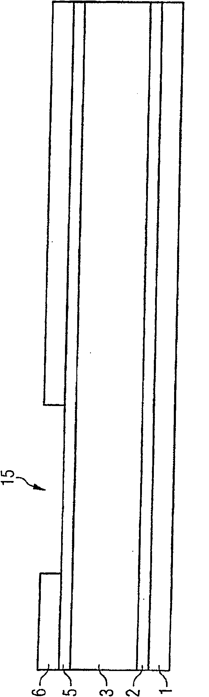
[0028] figure 2 A metal track stack is shown with a Ti glue layer 2, an AlCu interconnect 3, and an anti-reflective coating (ARC) layer 5, as used in the known art. In this example, the interconnection 3 is also intended to function as a lower MIM electrode, having a dielectric auxiliary layer 6 of about 50 to 100 nm thickness, for example made of SiO 2 or Si 3 N 4 The fabricator is deposited on top of the metal track stack 2, 3, 4 by using procedures known to be suitable for metallization, as part of a sacrificial layer rather than acting as a MIM dielectric, But rather, it will become part of the intermetal dielectric (IMD) that will be applied subsequently. Then, using known lithography and etching methods, the dielectric assist layer is removed at location 15, where a MIM capacitor is intended to be integrated.

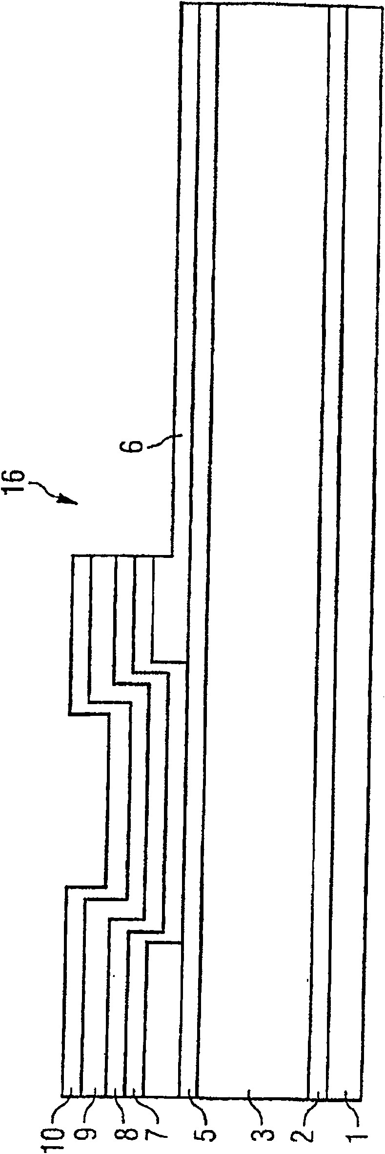
[0029] image 3 The MIM capacitor is shown after deposition and etching of the MIM dielectric 7 and the upper electrodes 8, 9, 10 have been performed. Now,...


PUM


Abstract

To fabricate an integrated semiconductor product with integrated metal-insulator-metal capacitor, first of all a dielectric auxiliary layer (6) is deposited on a first electrode (2, 3, 5). This auxiliary layer (6) is then opened up (15) via the first electrode. Then, a dielectric layer (7) is produced, and the metal track stack (8, 9, 10) for the second electrode is then applied to the dielectric layer (6). This is followed by the patterning of the metal-insulator-metal capacitor using known etching processes. This makes it possible to produce dielectric capacitor layers of any desired thickness using materials which can be selected as desired. In particular, this has the advantage that via etches can be carried out significantly more easily than in the prior art, since it is not necessary to etch through the residual dielectric capacitor layer above the metal tracks.

Description

technical field [0001] The present invention relates to an integrated semiconductor product having interconnects and a metal-insulator-metal capacitor. In particular, the invention relates to an integrated semiconductor product having interconnects comprising aluminum as an essential structural component. Background technique [0002] High-frequency circuits in BIPOLAR, BICMOS, and CMOS technologies require integrated capacitors with a high voltage linearity, accurately settable capacitance, and especially low parasitic capacitance, but these have been The known MOS or MIS capacitors used so far have an unsatisfactory voltage linearity due to the voltage-induced space charge regions, and the short distance from the substrate also bears numerous parasitic capacitances value. [0003] These difficulties can be avoided by using what are known as metal-insulator-metal capacitors (MIM capacitors), which are usually arranged between two metal layers and are thus located at a grea...

Claims


Application Information

Patent Timeline
Patent Type & Authority Patents(China)
IPC IPC(8): H01L21/02H01L29/92H01L21/768H01G4/12H01G4/08
CPCH01L21/76838H01L28/75H01L28/55H01L23/5223H01L23/5226
Inventor K·科勒H·克尔纳M·施伦克
Owner INFINEON TECH AG
Features
  • Generate Ideas
  • Intellectual Property
  • Life Sciences
  • Materials
  • Tech Scout
  • Unparalleled Data Quality
  • Higher Quality Content
  • 60% Fewer Hallucinations
Learn More