Supercharge Your Innovation With Domain-Expert AI Agents!

Inductive and capacitive coupling balancing electrical connector

A technology of inductive coupling and junction box, applied in the field of junction box, can solve the problems of high manufacturing process cost, phase change, long contact, etc., and achieve the effect of multi-design adaptability

Inactive Publication Date: 2010-02-03
PANDUIT
View PDF8 Cites 1 Cited by
  • Summary
  • Abstract
  • Description
  • Claims
  • Application Information

AI Technical Summary

Problems solved by technology

However, the manufacturing process required to produce contacts with specific lengths and orientations is costly
Furthermore, such contacts are already relatively long, which causes excessive phase transitions at high frequencies
Furthermore, the inductance between such contacts tends to vary excessively

Method used


Image

  • Inductive and capacitive coupling balancing electrical connector
  • Inductive and capacitive coupling balancing electrical connector
  • Inductive and capacitive coupling balancing electrical connector

Examples


Embodiment Construction

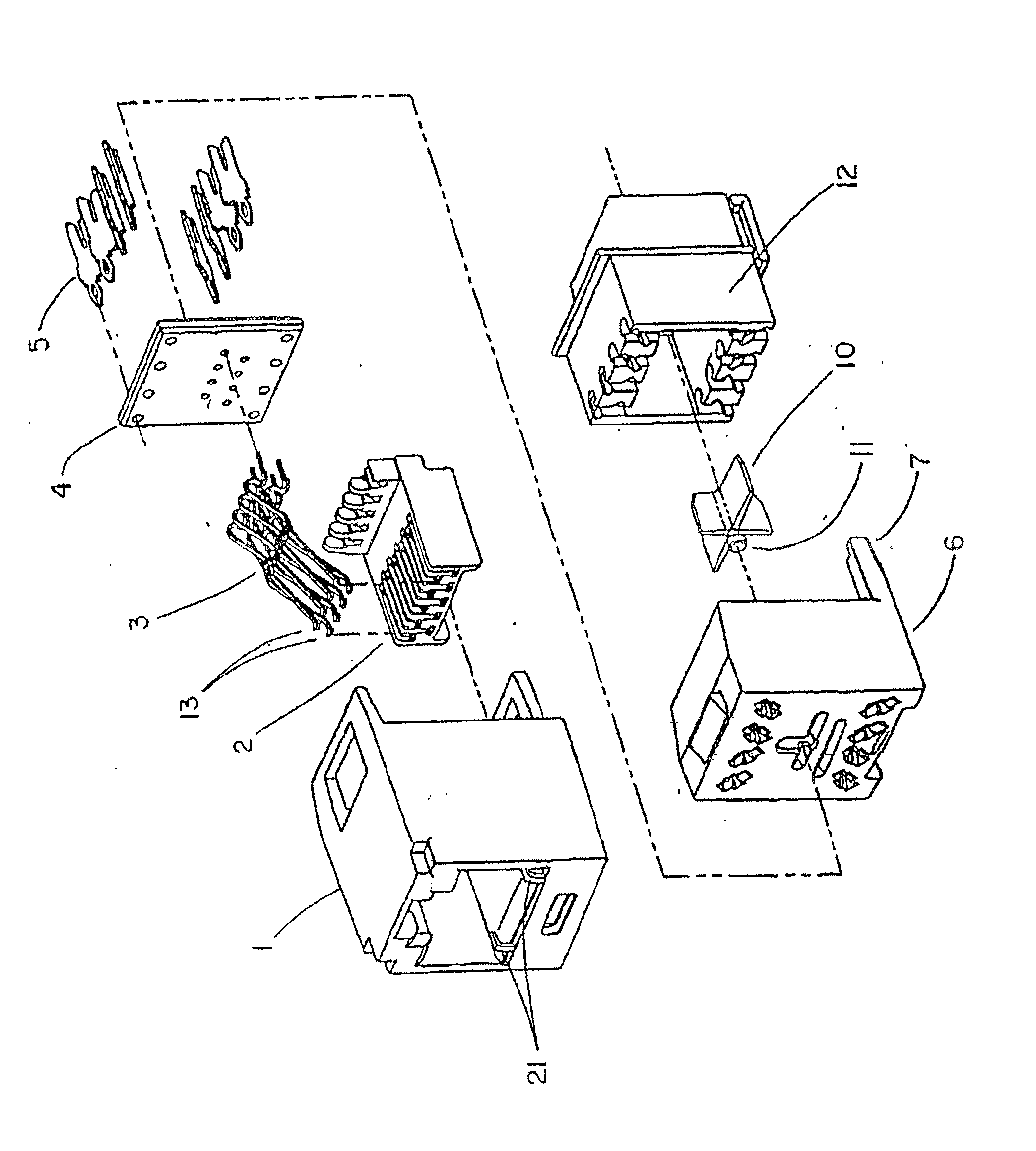
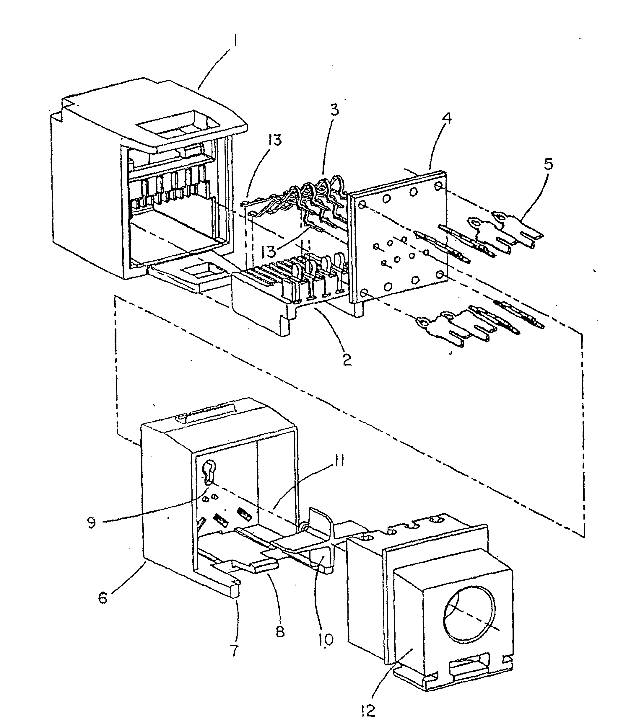
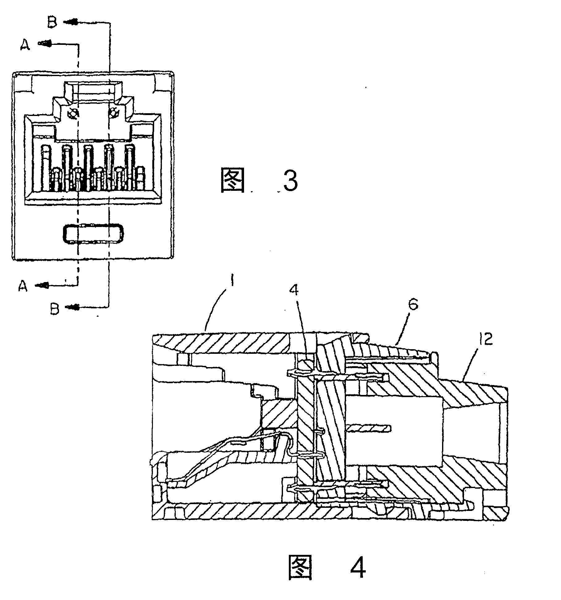
[0046] Figure 1-7 Shown is a junction box that can utilize a coupling balance circuit board according to the invention. From the exploded view ( figure 1 with figure 2 ) looking to the rear, there is the main housing 1 and the contact bracket 2 for the eight contacts 3 supported thereon. The contacts preferably engage the PCB 4 from the front through holes, and the eight IDCs 5 engage it from the rear in the same way. The rear housing 6, preferably with a pair of rails 7, includes a channel for the IDC, and the wiring cover 12 may preferably include a quarter pair spacer 10 for separating the individual wiring pairs therein. Unshielded twisted pairs in this area typically have varying amounts of twist depending on the manual installation process. Shielded twisted pairs in this area usually have a variable amount of shielding, depending on the manual installation process. Spacers eliminate crosstalk coupling between pairs in this area. The spacer 10 may include a mount...


PUM


Abstract

A network cable jack includes a printed circuit board (PCB) for balancing both inductive and capacitive coupling. Using a PCB allows compact trace paths to be formed without significantly increasing manufacturing costs. By including on each trace path two distinct inductance zones separated by a neutral zone, significant gains in degrees of freedom are achieved for designing PCB trace patterns inwhich a pair of inductive coupling zones jointly offset the inductive coupling caused by a specification plug and the jack contacts, both in magnitude and phase angle. Further, using distinct inductance zones offers more freedom regarding the placement of capacitive plates for use in capacitance balancing as well as the placement of terminals and insulation displacement contacts. Although the magnitude of a capacitive coupling is determined by the length of the capacitor plates parallel to current carrying traces, the approach allows capacitive and inductive coupling to be balanced independently.

Description

[0001] References to related applications [0002] This application claims priority to U.S. Provisional Application No. 60 / 531,756, filed December 22, 2003, entitled "Junction Box for Inductive and Capacitive Coupling Balancing," Attorney Ref. No. LCB447, by reference in its entirety content and all material referenced therein. In addition, this application refers in its entirety to US Patent 5,997,358, filed September 2, 1997, entitled "Junction Box with Delayed Signal Compensation," and all material cited therein. technical field [0003] The present invention relates generally to a junction box, and more particularly to a junction box having improved inductive and capacitive coupling balance characteristics. Background technique [0004] There has always been a desire to improve the electrical performance of a particular component or the overall system by minimizing crosstalk. Both near-end crosstalk (NEXT) and far-end crosstalk (FEXT) are weakened when the network ind...

Claims


Application Information

Patent Timeline
IPC IPC(8): H01R24/04H01R13/66H01R24/00H01R24/58H05K1/02H05K1/16
CPCH01R13/6469H01R4/2433H05K1/0228Y10S439/941H05K2201/10189H01R13/6658H05K1/165H01R23/005H01R24/64H01R13/6466H01R13/665H05K2201/09236H05K2201/09672H05K1/162Y10T29/49204Y10T29/49201Y10T29/49208Y10T29/49202Y10S439/942H01R4/2416
Inventor J·E·卡弗尼S·莱斯尼亚克
Owner PANDUIT
Features
  • R&D
  • Intellectual Property
  • Life Sciences
  • Materials
  • Tech Scout
  • Unparalleled Data Quality
  • Higher Quality Content
  • 60% Fewer Hallucinations
Learn More