

Chip package structure
A chip packaging and chip technology, applied in the direction of electrical components, electrical solid devices, circuits, etc., can solve the problems of contamination of the electrical connection area of the bonding wire, transportation or storage, and the way that circuit substrates cannot be stacked.
- Summary
- Abstract
- Description
- Claims
- Application Information
AI Technical Summary
Problems solved by technology
Method used
Image

Examples
no. 1 example
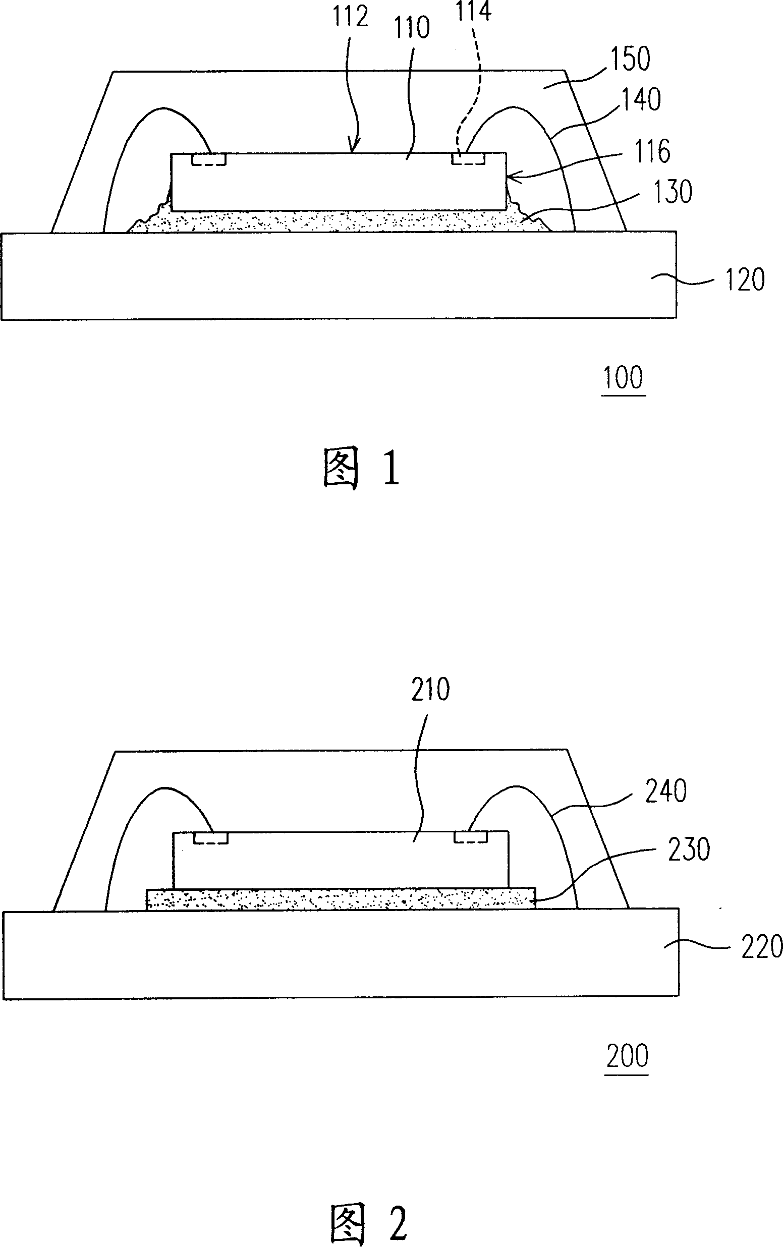
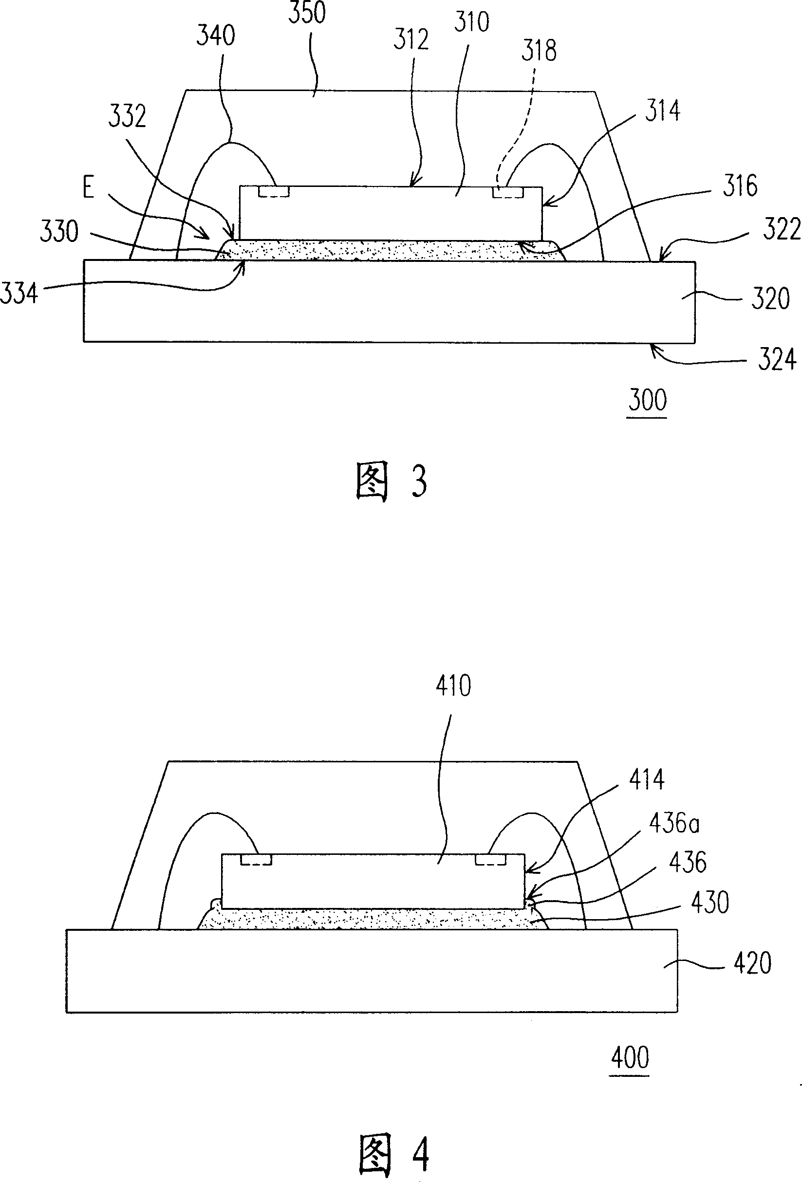
[0081] Please refer to FIG. 3 , which is a schematic cross-sectional view of a chip package structure according to a first embodiment of the present invention. The chip packaging structure 300 of the first embodiment includes a first chip 310 , a circuit substrate 320 and a two-stage thermosetting adhesive layer 330 . The first chip 310 has a first upper surface 312, a first side 314 and a first lower surface 316, the circuit substrate 320 has a substrate upper surface 322 and a substrate lower surface 324, and the first chip 310 and the circuit substrate 320 Phase electrical connection. In addition, a two-stage thermosetting adhesive layer 330 is located on the upper surface 322 of the substrate. The two-stage thermosetting adhesive layer 330 has a first adhesive surface 332 and a second adhesive surface 334, and part of the first adhesive surface 332 is bonded to the first lower surface 316. , the second adhesive surface 334 is bonded to the upper surface 322 of the substra...
no. 2 example
[0087] Please refer to FIG. 4 , which is a schematic cross-sectional view of a chip package structure according to a second embodiment of the present invention. The main difference between the second embodiment and the first embodiment lies in that the shape of the two-stage thermosetting adhesive layer 430 of the chip packaging structure 400 is different. The two-stage thermosetting adhesive layer 430 further includes an annular protrusion 436 surrounding the periphery of the first side 414, and the first side 414 is joined to the annular protrusion 436, and the annular protrusion 436 adjacent to the first side 414 A top surface 436a is substantially perpendicular to the first side 414 .
[0088] The reason for the formation of the ring-shaped protrusion 436 is the progress time of the two-stage thermosetting adhesive layer 430 from the state of the A-stage thermosetting adhesive layer to the state of the B-stage thermosetting adhesive layer. If the time at a certain designe...
no. 3 example
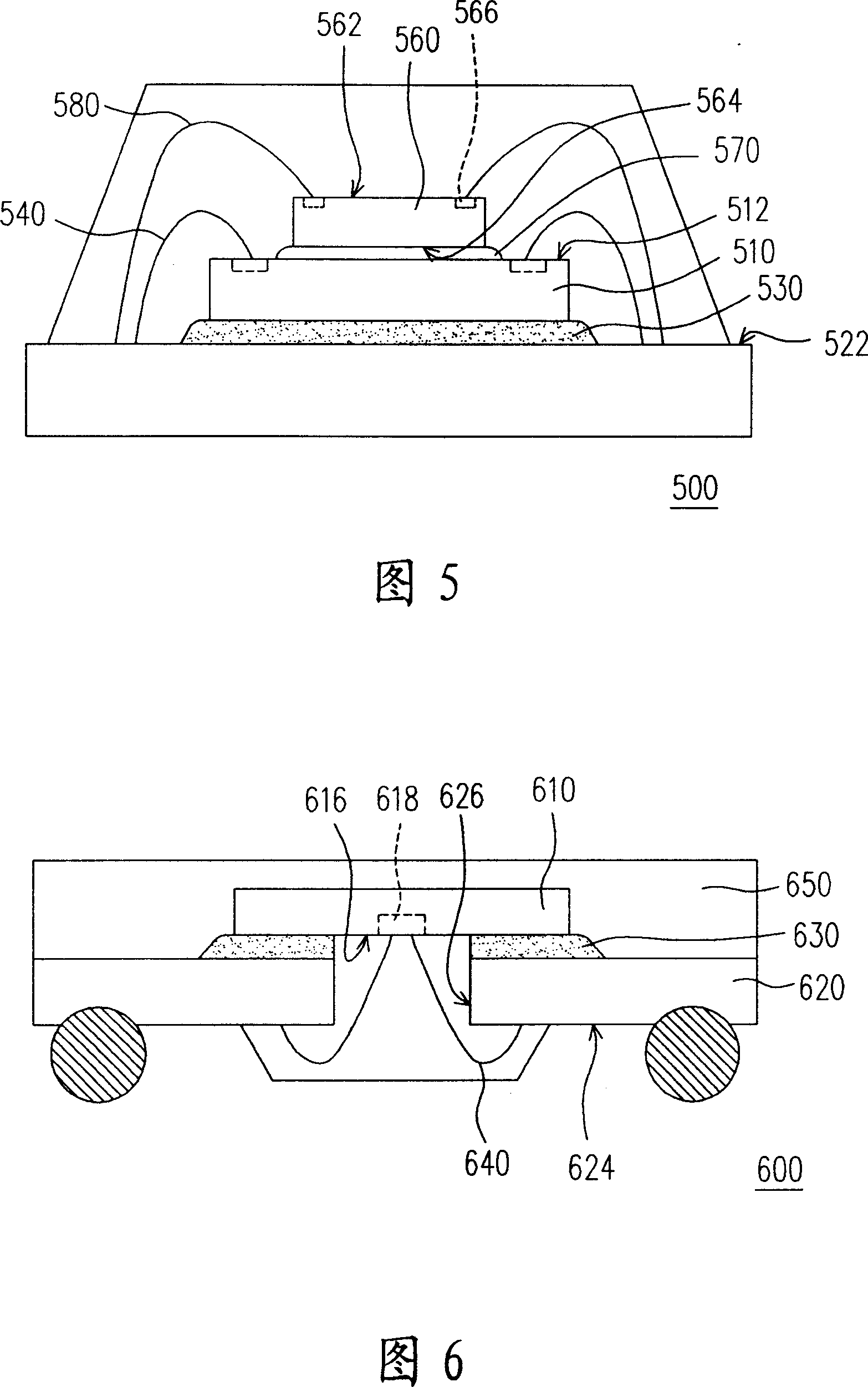
[0090] Please refer to FIG. 5 , which is a schematic cross-sectional view of a chip package structure according to a third embodiment of the present invention. The main difference between the third embodiment and the above-mentioned embodiments is that the chip package structure 500 is a multi-chip package structure, which further includes a second chip 560 and an adhesive layer 570 . The second chip 560 has a second upper surface 562 , a second lower surface 564 and a plurality of bonding pads 566 on the second upper surface 562 . The material of the adhesive layer 570 can be the same as that of the two-stage thermosetting adhesive layer 530. The adhesive layer 570 is disposed between the first wafer 510 and the second wafer 560, wherein the second lower surface 564 of the second wafer 560 is connected to the second wafer 560 by the adhesive layer 570. The first upper surface 512 of the first wafer 510 is bonded. In addition, the chip package structure 500 further includes a...
PUM
 Abstract
Description
Claims
Application Information