Supercharge Your Innovation With Domain-Expert AI Agents!

Manufacturing method of semiconductor device

一种制造方法、半导体的技术,应用在曝光领域,能够解决抗蚀剂膜抗蚀图形劣化、易产生缺陷、相对移动轨迹残留等问题

Inactive Publication Date: 2007-07-25
KK TOSHIBA
View PDF2 Cites 8 Cited by
  • Summary
  • Abstract
  • Description
  • Claims
  • Application Information

AI Technical Summary

Problems solved by technology

[0008] However, if the stage is simply moved quickly, droplets of the liquid immersion liquid tend to remain on the exposed substrate along the projection optical system of the exposure device and the relative movement track of the liquid immersion liquid with respect to the exposed substrate.
If droplets of the immersion liquid remain on the substrate to be exposed, the resist pattern formed on the resist film deteriorates and defects are likely to occur.
Furthermore, semiconductor devices manufactured based on resist patterns having such defects are more likely to be degraded in performance, quality, or reliability.

Method used


Image

  • Manufacturing method of semiconductor device
  • Manufacturing method of semiconductor device
  • Manufacturing method of semiconductor device

Examples


no. 1 Embodiment approach

[0028] First, a first embodiment according to the present invention will be described with reference to FIGS. 1 to 11 . In this embodiment mode, a method for forming a resist pattern is described, which can suppress or reduce the possibility of defects in the resist pattern in a liquid immersion exposure technique in which a partial region on a substrate exposes a pattern through a liquid film. The specific description will be given below.

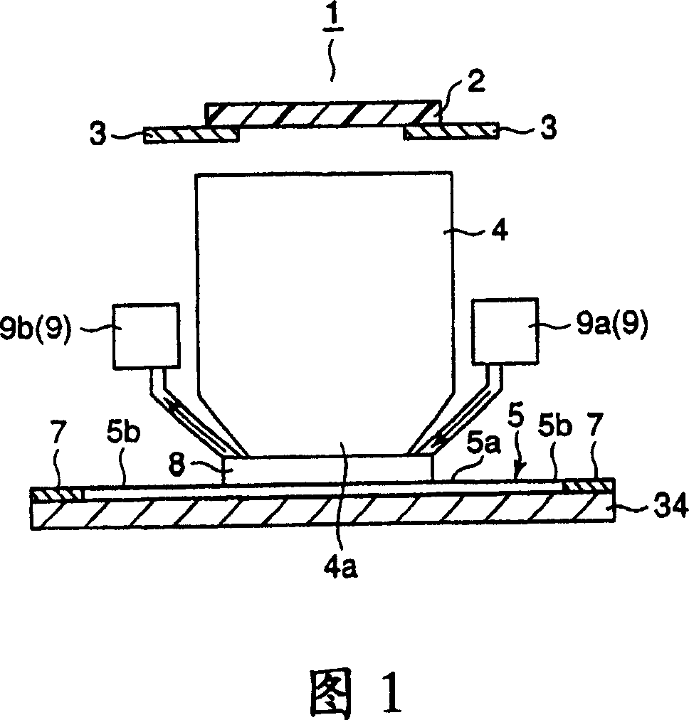
[0029] First, an exposure apparatus 1 according to the present invention will be described with reference to FIG. 1 . FIG. 1 is a schematic diagram showing a schematic configuration of an exposure apparatus 1 that performs exposure processing according to the present embodiment. The exposure apparatus 1 shown in FIG. 1 is a liquid immersion type exposure apparatus that performs so-called liquid immersion exposure, and performs exposure while a liquid is interposed between a substrate 5 to be exposed and the projection optical system 4 of ...

no. 2 Embodiment approach

[0097] Next, a second embodiment of the present invention will be described with reference to FIG. 12 . FIG. 12 is a plan view showing the relative movement trajectory of the liquid immersion head relative to the wafer in this embodiment according to each movement mode. In addition, the same code|symbol is attached|subjected to the same part as the said 1st Embodiment, and the detailed description is abbreviate|omitted.

[0098] In this embodiment, a technique for suppressing the generation of residual droplets by a method different from that of the first embodiment will be described. Specifically, in the second liquid immersion moving process, the longest moving distance in the same direction is calculated in consideration of the moving speed of the liquid immersion region 12 (stage 6), so that the liquid immersion region 12 (stage 6) is Zigzag movement is performed within the longest movement distance. Thereby, generation of residual liquid droplets is suppressed. A detai...

no. 3 Embodiment approach

[0104] Next, a third embodiment according to the present invention will be described with reference to FIG. 13 . FIG. 13 is a plan view showing the relative moving track of the liquid immersion head relative to the wafer in this embodiment according to each moving mode. In addition, the same code|symbol is attached|subjected to the same part as each of said 1st and 2nd embodiment, and the detailed description is abbreviate|omitted.

[0105] In the present embodiment, the liquid immersion area 12 not only passes through each exposure area 10 but also passes through the peripheral portion (outer edge portion, edge portion) 5b of the wafer 5 where the exposure area 10 is not set. In this case, it is also a technology that can suppress the generation of residual liquid droplets. Specifically, when the liquid immersion region 12 passes the edge portion 5 b of the wafer 5 , the relative moving speed of the liquid immersion region 12 with respect to the wafer 5 is decelerated. A de...


PUM


Abstract

A manufacturing method of a semiconductor device including a liquid immersion movement exposure of interposing a liquid between an exposure target substrate and a projection optical system of an exposure apparatus, and carrying out an exposure processing with respect to a plurality of exposure regions set on a surface of the substrate while relatively moving the substrate with respect to the system; a first liquid immersion movement of relatively moving the substrate with respect to the system while interposing the liquid between the substrate and the system and not executing exposure processing, in adjacent exposure regions of said each exposure region; and a second liquid immersion movement of relatively moving the substrate with respect to the system at a speed lower than a movement speed in the first movement, while interposing the liquid between the substrate and the system and not executing the exposure processing, in a distance that is longer than a movement distance in the first movement.

Description

[0001] Cross References to Related Applications [0002] This application is based on and claims priority from Japanese Patent Application No. 2006-012653 filed on January 20, 2006, and the entire content of this original patent application is hereby incorporated by reference. technical field [0003] The present invention relates to exposure technology in photolithography used in the manufacturing process of semiconductor devices, and more particularly to the exposure technology of semiconductor devices in which the exposure process is performed with a liquid interposed between the projection optical system of the exposure device and the substrate to be processed to be exposed. Manufacturing method. Background technique [0004] Recently, an exposure method called a liquid immersion exposure method has attracted attention. In this liquid immersion exposure method, liquid (immersion liquid) is filled between the projection optical system (projection lens) of the exposure de...

Claims


Application Information

Patent Timeline
Patent Type & Authority Applications(China)
IPC IPC(8): G03F7/20H01L21/00
CPCG03F7/70341G03D3/08G03B27/42G03F7/2041
Inventor 伊藤信一松永健太郎河村大辅
Owner KK TOSHIBA
Features
  • R&D
  • Intellectual Property
  • Life Sciences
  • Materials
  • Tech Scout
  • Unparalleled Data Quality
  • Higher Quality Content
  • 60% Fewer Hallucinations
Learn More