Method and apparatus for parameter transformation analog signal multiplication

An analog signal and transformation technology, which is applied in the field of parameter transformation analog signal multiplication, can solve the problems of poor precision, complex structure, difficulty in taking into account high precision, high-speed response and wide linear range, etc.

Inactive Publication Date: 2007-08-08
姚侗
View PDF0 Cites 6 Cited by
  • Summary
  • Abstract
  • Description
  • Claims
  • Application Information

AI Technical Summary

Problems solved by technology

Analog multiplier has good transient response but poor accuracy
All of the above methods put forward high requirements on circuit-related compon...

Method used


Image

  • Method and apparatus for parameter transformation analog signal multiplication
  • Method and apparatus for parameter transformation analog signal multiplication
  • Method and apparatus for parameter transformation analog signal multiplication

Examples


Embodiment 1

[0095] Definition of terms and description of concepts:

[0096] Regarding switched impedance networks:

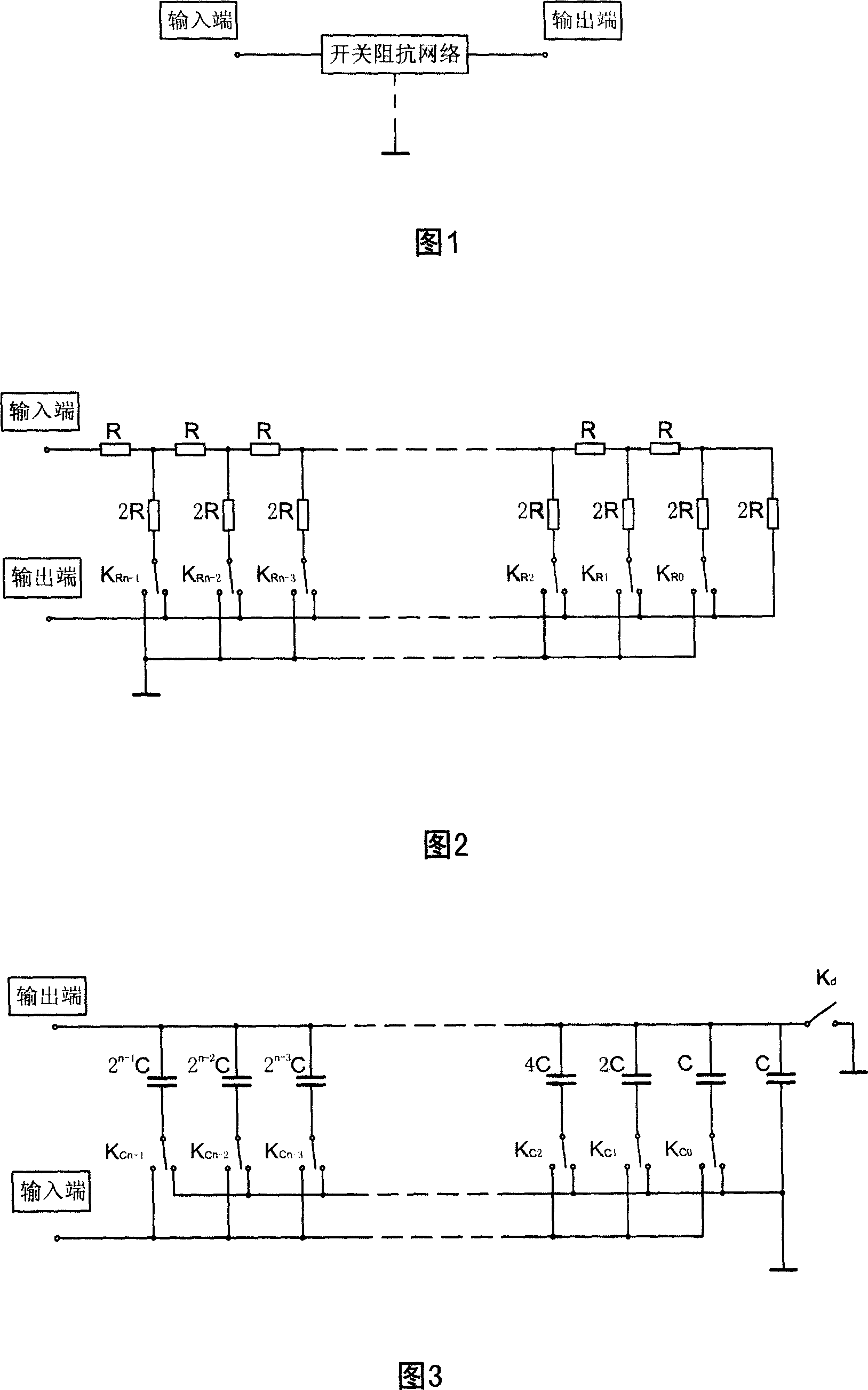
[0097] The switched impedance network of the present invention refers to a circuit formed by connecting impedance elements and switches, wherein all the switches can be controlled by external control signals. It has at least two external terminals—a signal input terminal and a signal output terminal, as shown in Figure 1 (the dotted ground line in the figure indicates that some switch impedance networks have ground terminals, and some switch impedance networks have no ground terminals).

[0098] The working process of the switch impedance network is divided into three stages in sequence: ①Input preparation stage: At this time, all switches in the network are in a combined state of "input preparation", and at this stage, the circuit is achieved by setting the data switch state. The required network state, ② signal input stage: At this time, all switches in the network are ...

Embodiment 2

[0137] Network input electrical parameter P i , the network output electrical parameter P o And the electrical parameter P to be multiplied i1 and P i2 Both may be current or voltage respectively. In order to simplify the description and combine common situations, the networks described in the following embodiments are all voltage input networks; the electrical parameter P to be multiplied i1 , P i2 and the reference electrical parameter P used j Both are voltages. That is, the reference electrical parameter P j =V j And the electrical parameter P to be multiplied i1 =V i1 ,P i2 =V i2 The implementation scheme of the case where both are voltages, for P i and P i1 ,P i2 and the rest of the current-input network can be obtained by simple changes from the embodiments given below. For this purpose, a reference voltage V j (>0, constant). The reference voltage V used in this patent j Both are positive voltage sources (i.e., V j >0), and is a ...

Embodiment 3

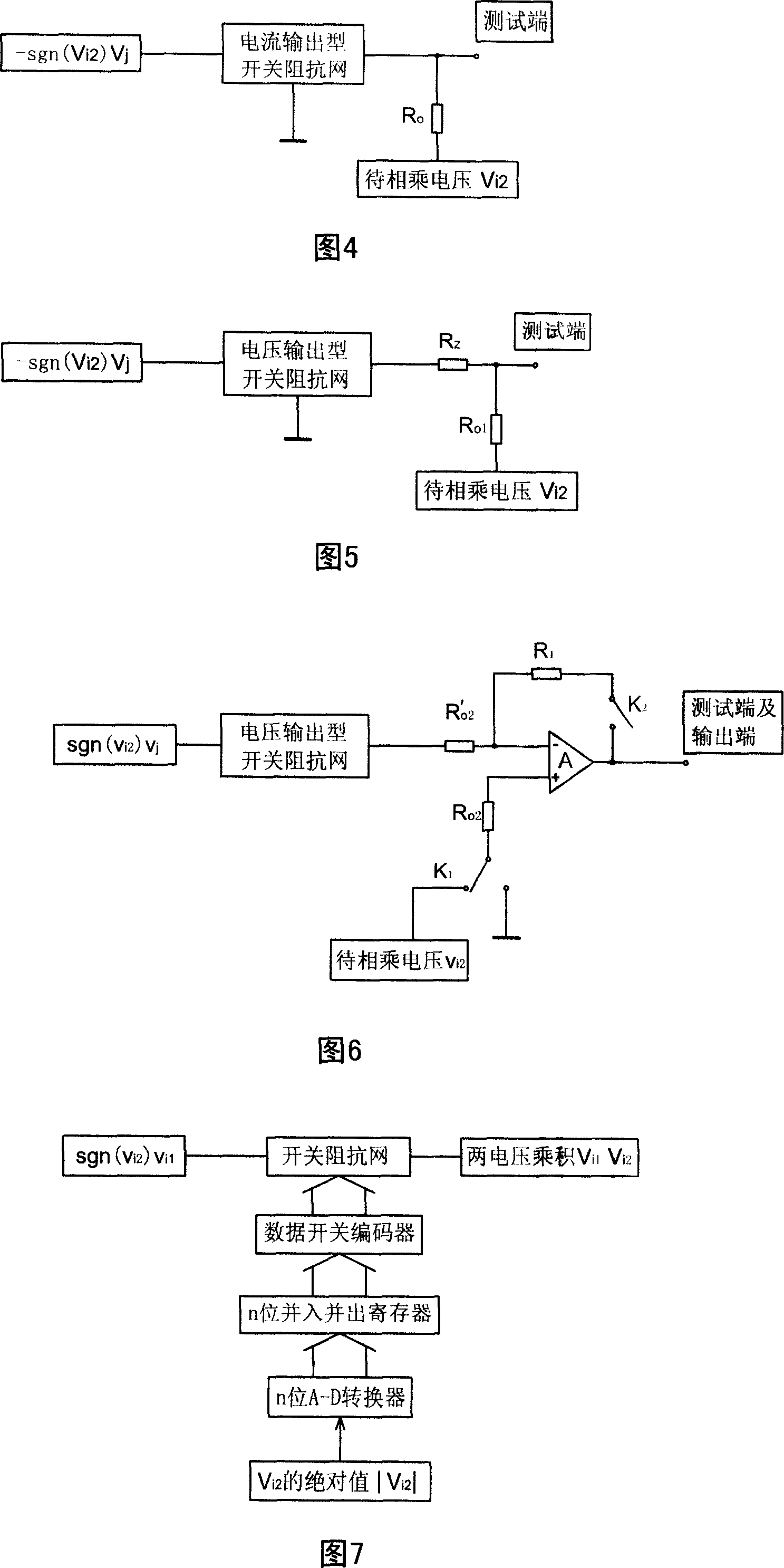
[0160] Introducing the reference voltage source V j , V j is a known constant. The network used is a current output network, and the tracking method used is the direct tracking four-quadrant multiplication described in the second embodiment. In this example η = I o V i The dimension is the guide Nano, connect a resistor R at the output of the network 0 , taking the network output as the test terminal. The basic process of this embodiment is simply described as: connecting the voltage-sgn(V i2 )V j , in R 0 Floating terminal access voltage V i2 ,As shown in Figure 4. Adjust the data switch in the network according to whether the test terminal voltage is positive or negative until the test terminal voltage is zero (in fact, the absolute value of the test terminal voltage is the smallest, which will not be explained later),

[0161] At ...


PUM


Abstract

The invention is about parameters transformed analog signal multiplication method and corresponding instruments especially for a pair of analog signals multiplication. The invention uses the linear network switch impedance characteristics and the precise nature of controllable network transfer coefficient about impedance characteristics through the eta = Po / Pi (Pi and Po are respectively network input and output parameters) to maintain proportionate real-time with absolute parameters of Pi2 | Pi2 |, eta = a | Pi2 | (a normal volume); meanwhile, it access to the network with another signed parameters to be multiplied sgn (Vi2) Pi1, and we can get Po eta = sgn (Vi2) Pi1 = aPi1 Pi2 through the output of network. It makes the multiplication operation with high-precision, high-speed response and wide linear range. The invention with simple structure lowers requirements for the circuit components and makes the entire multiplier integrated in a chip with very favorable conditions.

Description

technical field [0001] The invention relates to a method and a device for multiplication of analog signals with parameter conversion, which is a calculation method and device for analog signals, and in particular to a method and device for multiplication of analog signals. Background technique [0002] The known analog voltage V i1 , V i2 The product of is mainly used in the following ways: for V i1 , V i2 At the same time, digital sampling is carried out, and then sent to the digital multiplier to obtain the digital product, and then the analog product V is obtained by digital-to-analog conversion i1 V i2 . Simulate a multiplier using log-antilog. Use V i1 , V i2 Perform double modulation on the voltage-frequency converter to obtain the number of pulses per unit time as V i1 , V i2 The product. Variable transconductance multiplier. Digital multipliers can multiply very accurately, but the response speed is not satisfactory. Analog multipliers have good transien...

Claims


Application Information

Patent Timeline
IPC IPC(8): G06G7/163H03H7/00
Inventor 姚侗
Owner 姚侗
Why Eureka
Try Eureka