

Semiconductor device
A semiconductor and transistor technology, applied in the field of preventing electrostatic damage, can solve the problems of PN junction damage, easy local concentration of surge current, etc., and achieve good ohmic contact effect
- Summary
- Abstract
- Description
- Claims
- Application Information
AI Technical Summary
Problems solved by technology
Method used
Image

Examples
no. 1 Embodiment approach
[0044] Below, refer to Figure 6 ~ Figure 9 A first embodiment of the semiconductor device of the present invention will be described.
[0045] First, a preferred example of the semiconductor device according to the embodiment will be described.
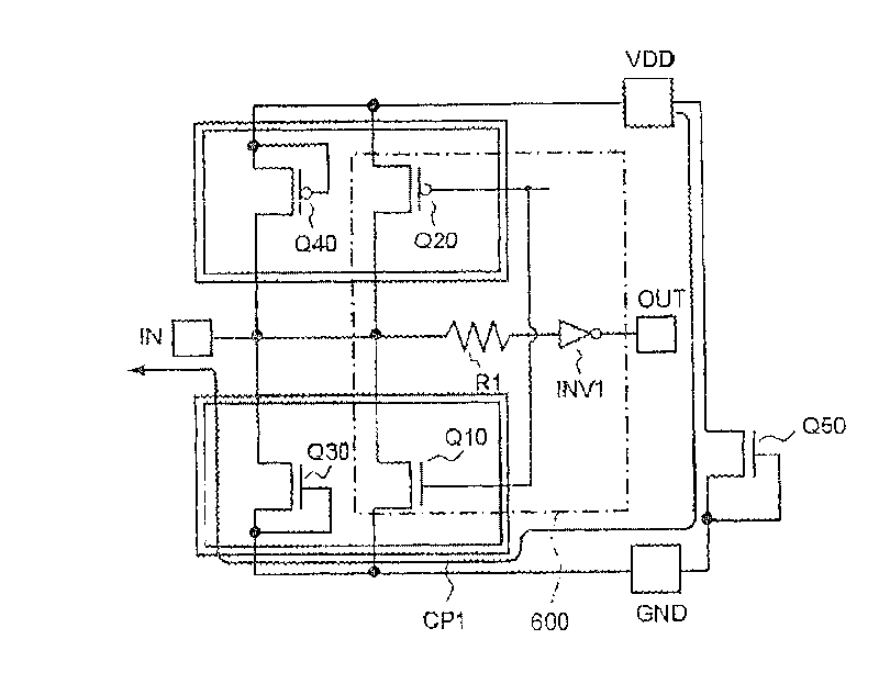
[0046] Image 6 It is a circuit diagram of the semiconductor device 10 (input-output circuit) on which the ESD protection circuit is mounted. Image 6 The shown semiconductor device 10 has: a CMOS output circuit 6 (output transistors Q1, Q2, current limiting resistor R1, inverter INV1) receiving a gate control signal; and a protection transistor ( Q3, Q4, Q5).
[0047] The NMOS transistor Q5 is provided between a power supply terminal VDD (second reference potential) and a ground terminal GND (first reference potential). The NMOS transistor Q3 is provided between the input terminal IN and the ground terminal GND, and the PMOS transistor Q4 is provided between the input terminal IN and the power supply terminal VDD.
[0048] Such...
no. 2 approach
[0081] Below, refer to Figure 10 ~ Figure 12 A second embodiment of the semiconductor device of the present invention will be described. In addition, the same reference numerals are assigned to the same parts as those of the semiconductor device of the first embodiment, and repeated explanations are omitted.
[0082] As already described, in the semiconductor device 10 according to the first embodiment, since no silicide is formed on the side facing the transistor formation region 20, the surge current is less likely to be locally concentrated as compared with the prior art. The purpose of the semiconductor device 11 of the present embodiment is to prevent the local concentration of the surge current more reliably by its structure.
[0083] First, the structure of the semiconductor device 11 of the embodiment will be described.
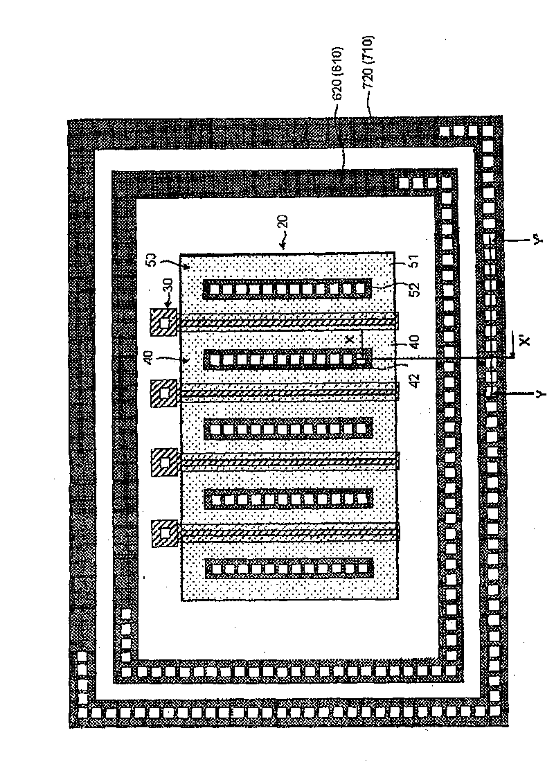
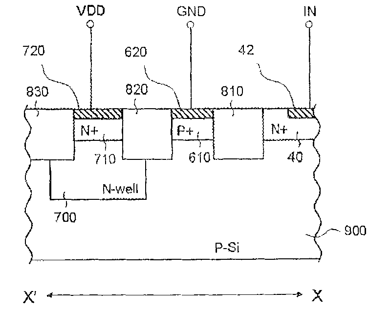
[0084] Figure 10 It is a plan view of the semiconductor device 11 of the second embodiment. Figure 11 is along Figure 10 A cross-sectional v...
no. 3 approach
[0095] Below, refer to Figure 13 to Figure 16 A third embodiment of the semiconductor device of the present invention will be described. In addition, the same reference numerals are assigned to the same parts as those of the semiconductor device of the first embodiment, and repeated explanations are omitted.
[0096] As already described, in the semiconductor device 10 of the first embodiment, since no silicide is formed on the side facing the transistor formation region 20, it is less likely to locally concentrate the surge current as compared with the prior art. The purpose of the semiconductor device 12 of the present embodiment is to prevent the local concentration of the surge current more reliably by its structure.
[0097] First, the structure of the semiconductor device 12 of the embodiment will be described.
[0098] Figure 13 It is a plan view of the semiconductor device 12 of the third embodiment. Figure 14 is along Figure 13 A cross-sectional view of the s...
PUM
 Abstract
Description
Claims
Application Information