Optoelectric composite substrate and electronic apparatus

A photoelectric composite and substrate technology, applied in circuits, lasers, electrical components, etc., can solve the problems of VCSEL chip size increase, collapse, and inability to convert laser into parallel light or concentrating light.

Inactive Publication Date: 2007-08-29
SEIKO EPSON CORP
View PDF0 Cites 10 Cited by
  • Summary
  • Abstract
  • Description
  • Claims
  • Application Information

AI Technical Summary

Problems solved by technology

In the Fraunhofer region, the laser can be shaped by lenses, etc., but in the Fresnel region, the laser cannot be converted into parallel light or concentrated light
Therefore, there is a restriction that the part where the microlens is formed must be separated from the light emitting part of the VCSEL by a certain distance (about 100 to 200 μm).
[0007] In view of the limitations of the above two points, when the planar area of ​​the VCSEL chip is about 500 μm, as disclosed in Non-Patent Document 1, the bottom area of ​​the mold part constituting the microlens cannot be taken as a sufficient area relative to its height.
Therefore, in the dicing process of cutting out each VCSEL from the substrate, damage such as bending, sagging, falling off, and bending of the mold part may occur, and it is not difficult to imagine that this will cause a decrease in manufacturing yield.
In order to prevent this damage, it should be enough to increase the bottom area of ​​the mold portion (the contact area with the substrate), but if the bottom area of ​​the mold portion is increased, the size of each VCSEL chip will be significantly increased, so that it can be obtained from one substrate. The number of VCSEL chips manufactured has been greatly reduced, resulting in an increase in manufacturing costs

Method used


Image

  • Optoelectric composite substrate and electronic apparatus
  • Optoelectric composite substrate and electronic apparatus
  • Optoelectric composite substrate and electronic apparatus

Examples


no. 1 approach

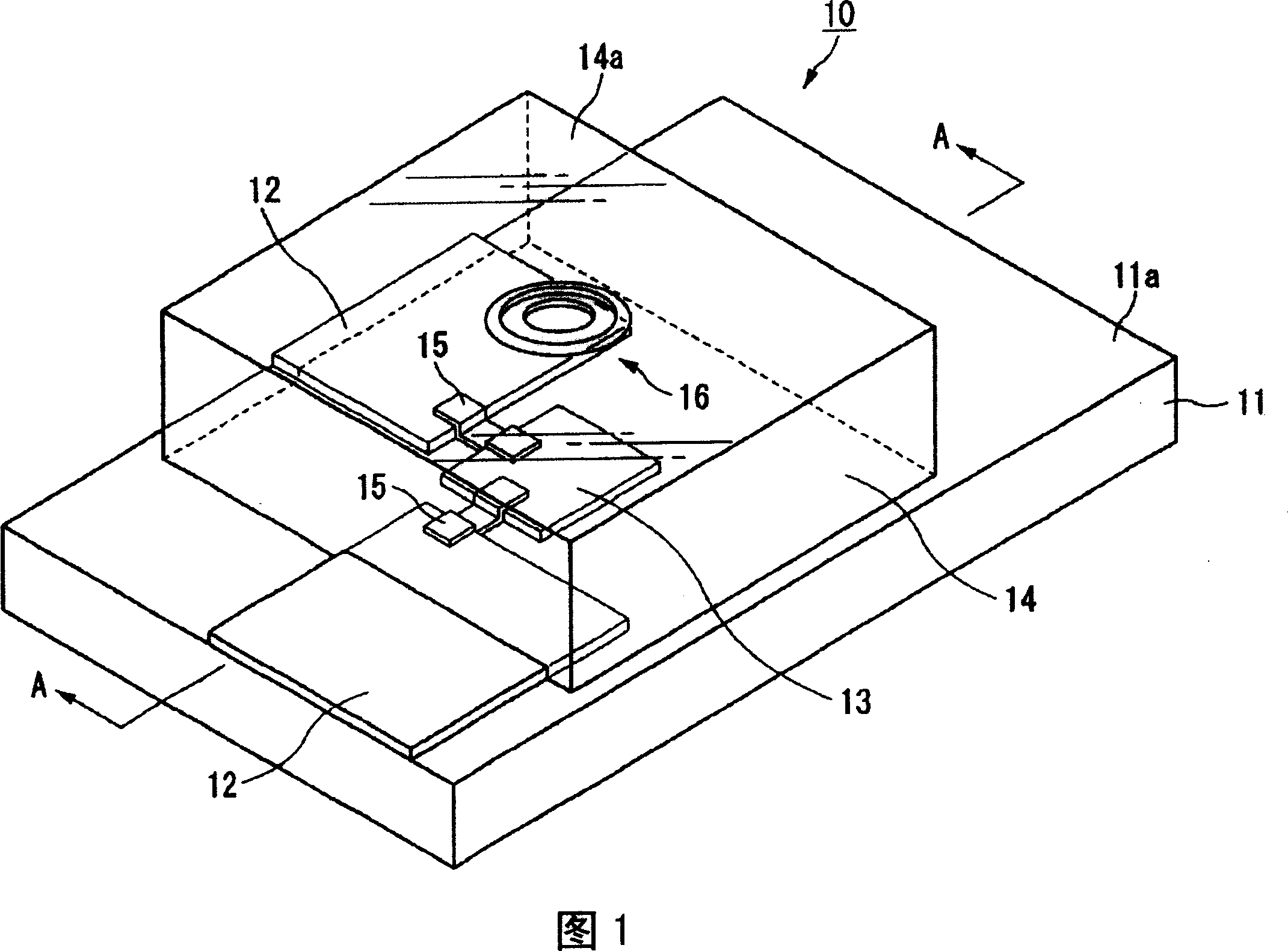
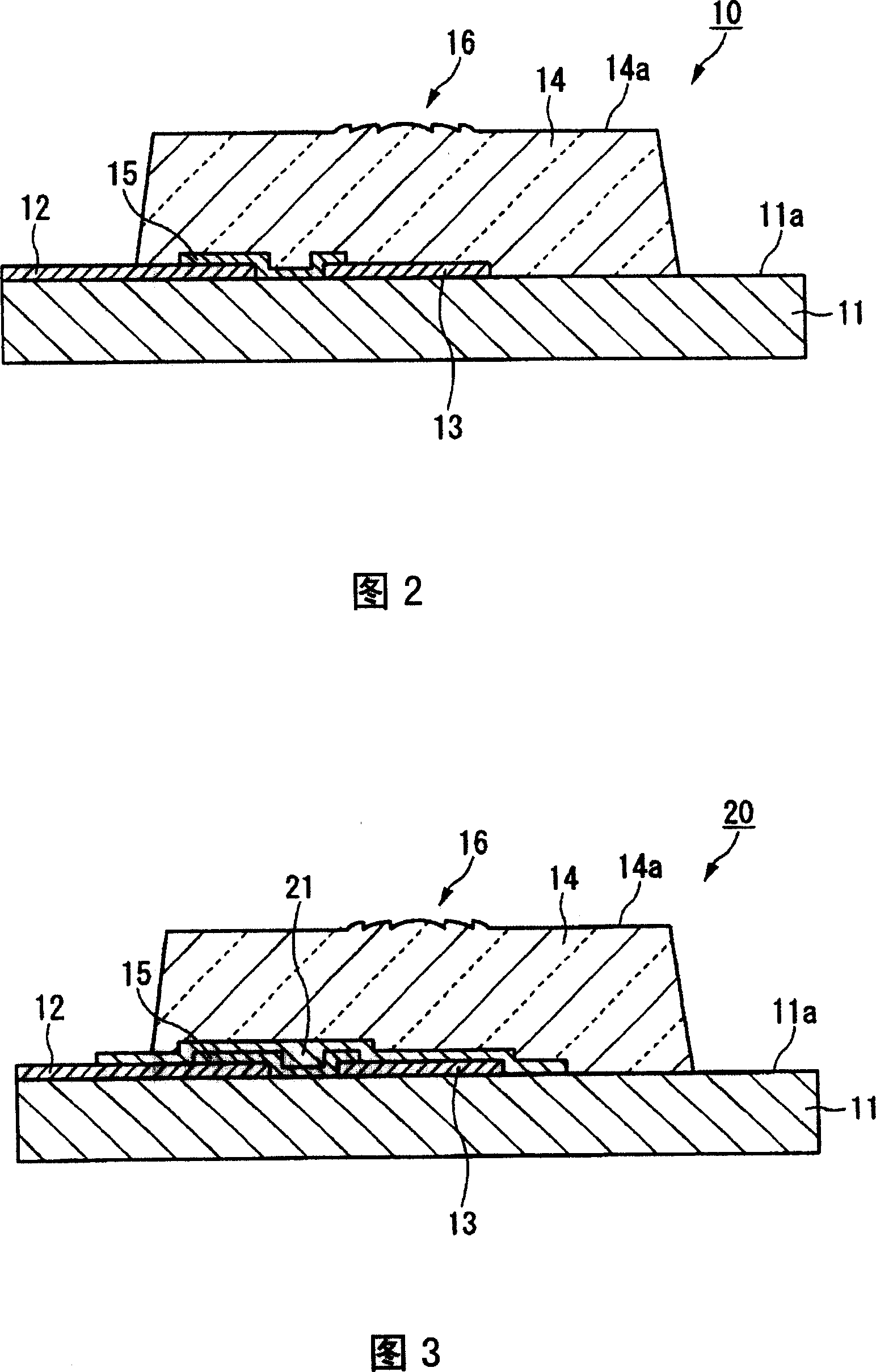
[0060] FIG. 1 is a perspective view showing main parts of an optoelectronic composite substrate 10 according to a first embodiment of the present invention, and FIG. 2 is a cross-sectional view taken along line A-A in FIG. 1 . As shown in FIGS. 1 and 2 , the photoelectric composite substrate 10 of this embodiment includes: a substrate 11 , a printed wiring 12 formed on the surface 11 a side of the substrate 11 , a thin optical element 13 mounted on the surface 11 a side of the substrate 11 , and The lens mold 14 is formed on the surface 11 a side of the substrate 11 so as to cover the thin optical element 13 . In addition, in this embodiment, a case where the photoelectric composite substrate 10 is a printed wiring board with little flexibility is described as an example, but a flexible FPC (flexible printed wiring board) may also be used.

[0061] For the substrate 11 , for example, a substrate made of at least phenolic resin or glass epoxy resin, a semiconductor substrate su...

no. 2 approach

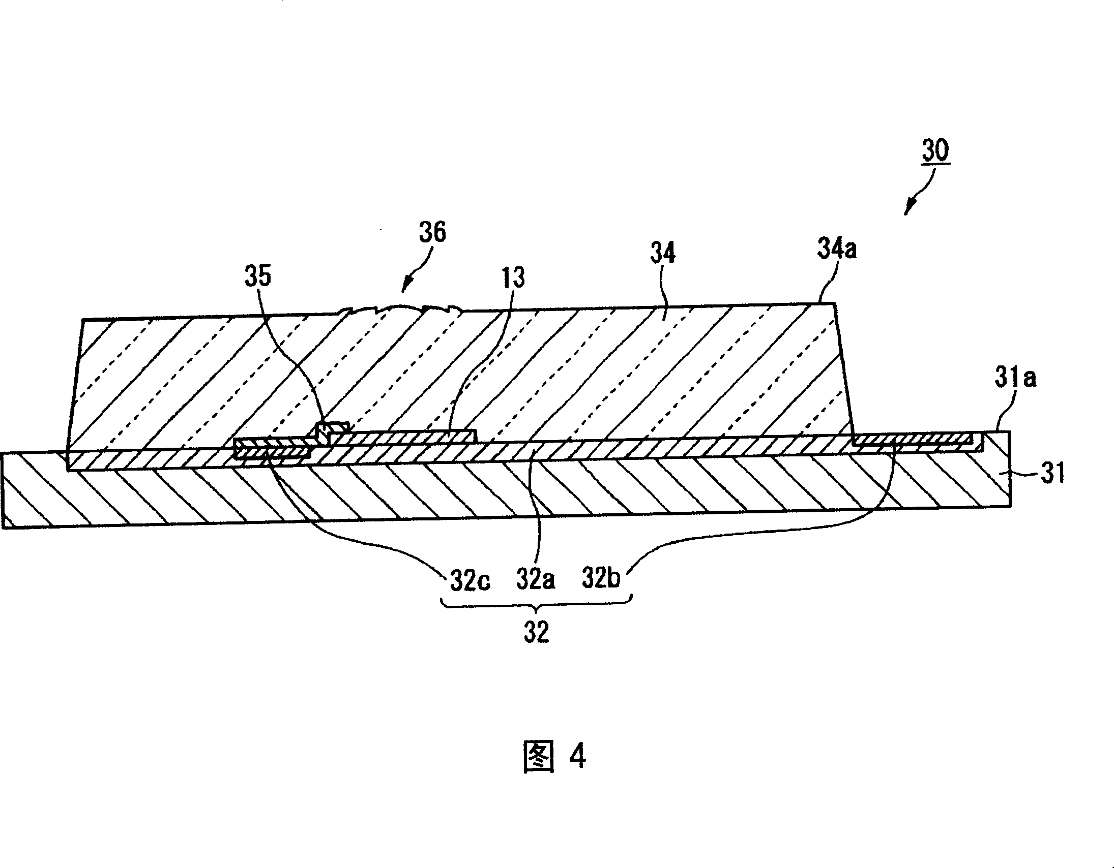
[0083] 4 is a cross-sectional view showing the main part of the photoelectric composite substrate 10 according to the second embodiment of the present invention, and the components corresponding to the configuration of the photoelectric composite substrate 10 according to the first embodiment described with reference to FIGS. 1 and 2 are indicated. same mark. As shown in FIG. 4 , the optoelectronic composite substrate 30 of this embodiment includes: a substrate 31 , a thin optical element 13 mounted on the surface 31 a side of the substrate 31 , and an The lens mold 34. In addition, in the example shown in FIG. 4, wiring equivalent to the printed wiring 12 included in the photoelectric composite substrate 10 shown in FIGS. side.

[0084] The substrate 31 is, for example, a semiconductor substrate such as a silicon substrate, and the circuit 32 related to the thin optical element 13 is formed on the side of the surface 31 a. The circuit 32 is constituted by at least a circui...

no. 3 approach

[0091] 5 is a cross-sectional view showing main parts of an optoelectronic composite substrate 30 according to a third embodiment of the present invention, and the same symbols are attached to components corresponding to those included in the optoelectronic composite substrate 30 according to the second embodiment described with reference to FIG. 4 . The photoelectric composite substrate 40 of the third embodiment shown in FIG. 5 is different from the photoelectric composite substrate 30 of the second embodiment shown in FIG. , corresponding to each of the thin optical elements 13, 43, lens elements 36a, 36b are formed on the surface 34a of the lens mold 34, respectively. In addition, in this embodiment, it is assumed that the thin optical element 13 is a light emitting element such as a VCSEL, and the thin optical element 43 is a light receiving element such as a PD.

[0092] In the circuit 32 formed on the surface 31a side of the substrate 31, in addition to the circuit part...


PUM


Abstract

The photoelectric composite substrate 10 comprises a substrate 11, a printed wiring 12 and a thin optical element 13 formed on a front surface 11a side of the substrate 11. The thin optical element 13 has an electrode formed on its front surface, allowing at least inputting / outputting of light from the front surface, and the rear surface of it is mounted on the substrate 11 by bonding it to the front surface 11a of the substrate 11. The thin optical element 13 is covered with a lens mold 14. In the lens mold 14, a lens element 16 that refracts the light inputted / outputted with the thin optical element 13 is formed in a Fraunhofer region of the light inputted / outputted with the thin optical element 13. So the invention provides a photoelectric composite substrate, along with electronic equipment equipped with it, capable of preventing degradation in manufacture yield due to damage on a mold part with no increase of a manufacturing cost.

Description

technical field [0001] The present invention relates to a photoelectric composite substrate including electrical wiring and a photoelectric conversion element, and electronic equipment including the photoelectric composite substrate. Background technique [0002] In recent years, optical communication, which uses optical signals to send and receive information, has been widely used. Compared with electrical communication that uses electrical signals to send and receive information, optical communication has advantages such as reduced signal attenuation, increased amount of processed information, and prevention of radiation of electromagnetic waves to the surroundings. In the past, optical communication was generally limited to medium and long-distance communications of hundreds of kilometers or more, but in recent years it has also been widely used in short-distance communications of several kilometers, and it is also used in distances of several meters. Information communi...

Claims


Application Information

Patent Timeline
Patent Type & Authority Applications(China)
IPC IPC(8): H01S5/022H01S5/183H01S5/00H01L31/00H01L33/00H01L21/02H01L33/54
Inventor 近藤贵幸
Owner SEIKO EPSON CORP
Why Eureka
Try Eureka