Grid-shaped electrostatic discharge protection device

An electrostatic discharge protection and grid-like technology, which is applied in the field of electrostatic discharge protection devices, can solve the problems that the voltage value of the trigger point cannot be adjusted flexibly and the anti-static effect is not very ideal, so as to increase the effective circulation area and flexibly The effect of adjusting and increasing the effective area

Inactive Publication Date: 2007-10-03
ZHEJIANG UNIV
View PDF0 Cites 1 Cited by
  • Summary
  • Abstract
  • Description
  • Claims
  • Application Information

AI Technical Summary

Problems solved by technology

However, the anti-static effect of the thyristor SCR in the harsh electrostatic environment is not very ideal, and the trigger point voltage value cannot be adjusted flexibly

Method used


Image

  • Grid-shaped electrostatic discharge protection device
  • Grid-shaped electrostatic discharge protection device
  • Grid-shaped electrostatic discharge protection device

Examples


Embodiment Construction

[0012] The present invention will be further described in conjunction with the drawings and embodiments of the description.

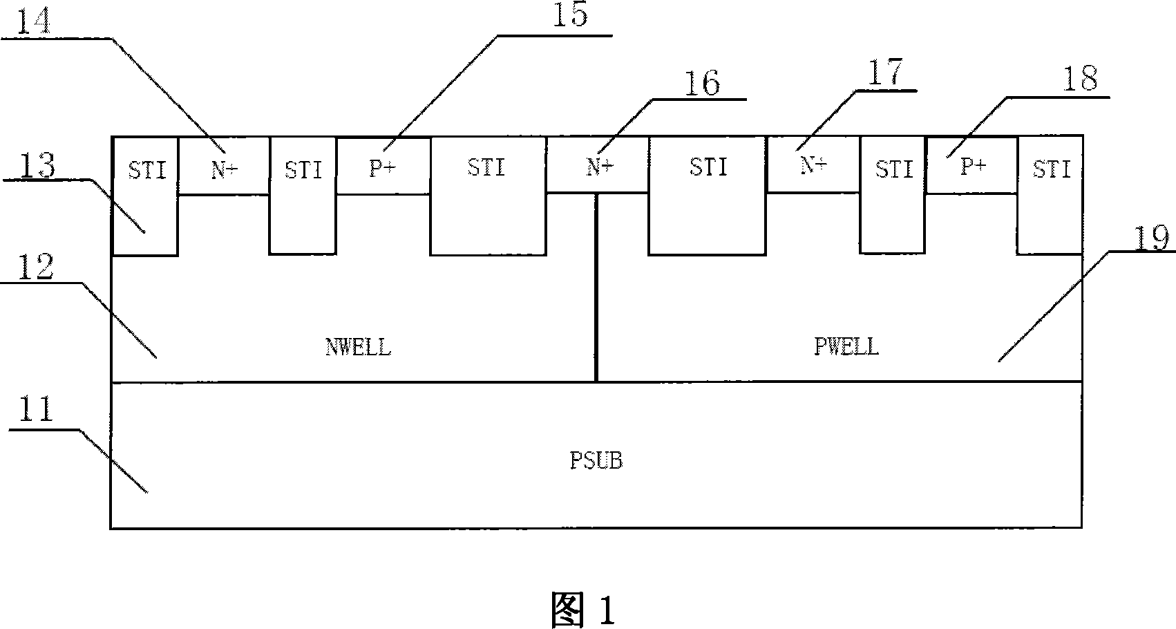
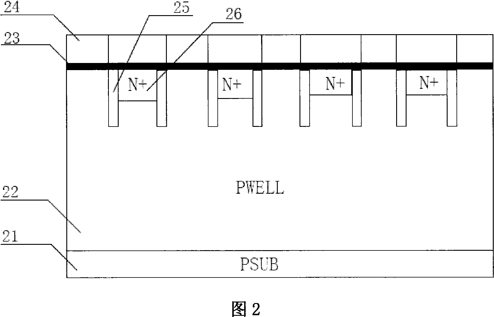
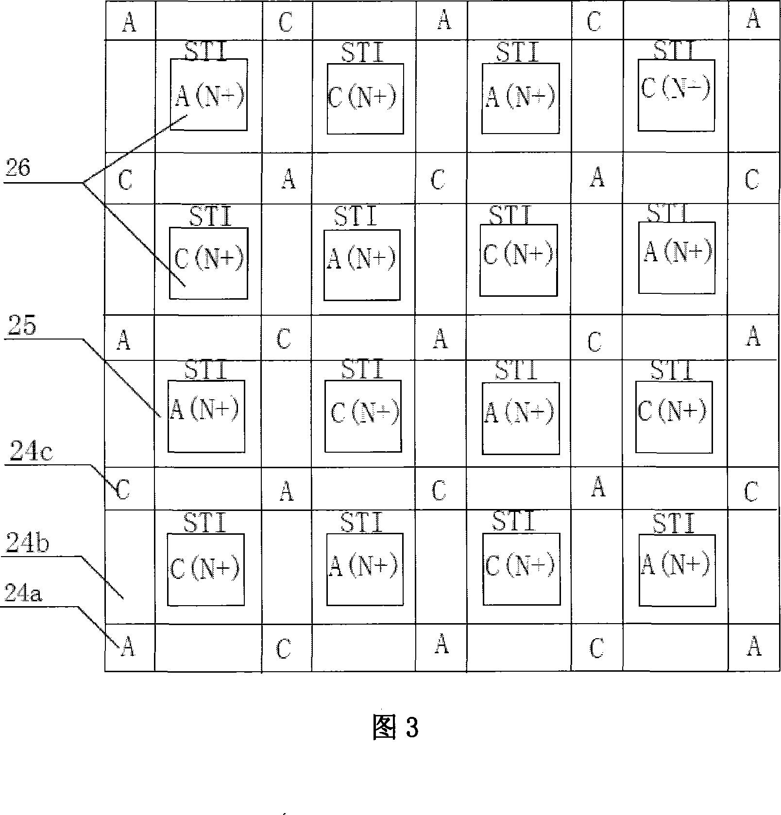
[0013] As shown in FIG. 2 and FIG. 3 , a grid-shaped electrostatic discharge protection device includes a P-type substrate 21 on which a P-well 22 is arranged. Above the P well 22 is a fishnet-shaped polysilicon region (24a, 24b, 24c), and just below the polysilicon region (24a, 24b, 24c) is a SiO2 region of the same shape. 2 Oxide layer 23, SiO 2 The lower surface of oxide layer 23 is in contact with the upper surface of P well 22 . The nodes (24a, 24c) of the fishnet-shaped polysilicon regions are doped with P-type impurities or N-type impurities to become P-type polysilicon regions 24a or N-type polysilicon regions 24c respectively, while adjacent nodes (P-type polysilicon regions 24a and N-type polysilicon regions 24a and N-type Intrinsic polysilicon regions 24b are provided between the polysilicon regions 24c). The P-type polysilicon region 24a ...


PUM


Abstract

The present invention relates to an electrostatic discharge protection device utilizing multicrystal silicon layout to hierarchically construct electrostatic current dumping channel. It is characterized by that in P trap on the P-type substrate N+injection zone several plane array arrangements is set, along peripheral side wall of every N+injection zone a shallow trench isolation STI with square-ring type is set, over P trap a grid-shaped multicrystal silicon layer is set, the inner wall of said grid is correspondent to the outer wall position of said shallow trench isolation STI. The grid node position of said multicrystal silicon layer is P-type multicrystal silicon zone or N-type multicrystal silicon zone, and between the multicrystal silicon layer and P-type substrate a SiO2 oxide layer is set.

Description

technical field [0001] The invention belongs to the technical field of integrated circuits, and in particular relates to an electrostatic discharge protection device which utilizes polysilicon layout layers to construct electrostatic current discharge channels. Background technique [0002] Electrostatic discharge is an instantaneous process in which a large amount of charge is poured into the integrated circuit from the outside to the inside when an integrated circuit is floating, and the whole process takes about 100ns. In addition, hundreds or even thousands of volts of high voltage will be generated when the integrated circuit is discharged, which will break through the gate oxide layer of the input stage in the integrated circuit. As the size of MOS transistors in integrated circuits is getting smaller and smaller, the thickness of the gate oxide layer is also getting thinner. Under this trend, high-performance electrostatic protection circuits are used to discharge ele...

Claims


Application Information

Patent Timeline
Patent Type & Authority Applications(China)
IPC IPC(8): H01L27/04H01L23/60
Inventor 霍明旭崔强韩雁刘俊杰董树荣黄大海徐向明
Owner ZHEJIANG UNIV
Why Eureka
Try Eureka