LED package structure and method for manufacturing the same

A technology for light-emitting diodes and packaging structures, which is applied in the manufacture of semiconductor/solid-state devices, electrical components, and electrical solid-state devices, etc., can solve the problems of low light extraction efficiency of light-emitting diodes and reduction of total light reflection.

Inactive Publication Date: 2007-10-03
CHI LIN OPTOELECTRONICS CO LTD
View PDF0 Cites 6 Cited by
  • Summary
  • Abstract
  • Description
  • Claims
  • Application Information

AI Technical Summary

Problems solved by technology

[0005] One aspect of the present invention provides a packaging structure of light-emitting diodes, by using a plasma chemical vapor deposition layer with a single-layer or multi-layer structure to substantially reduce the total reflection of light in the light-emitting diode chip, thereby solving the problem of light extraction of light-emitting diodes The problem of low efficiency

Method used


Image

  • LED package structure and method for manufacturing the same
  • LED package structure and method for manufacturing the same
  • LED package structure and method for manufacturing the same

Examples


Embodiment Construction

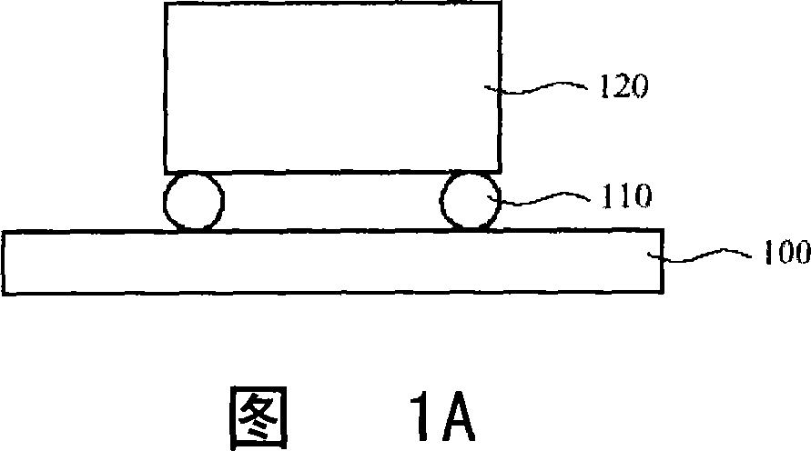
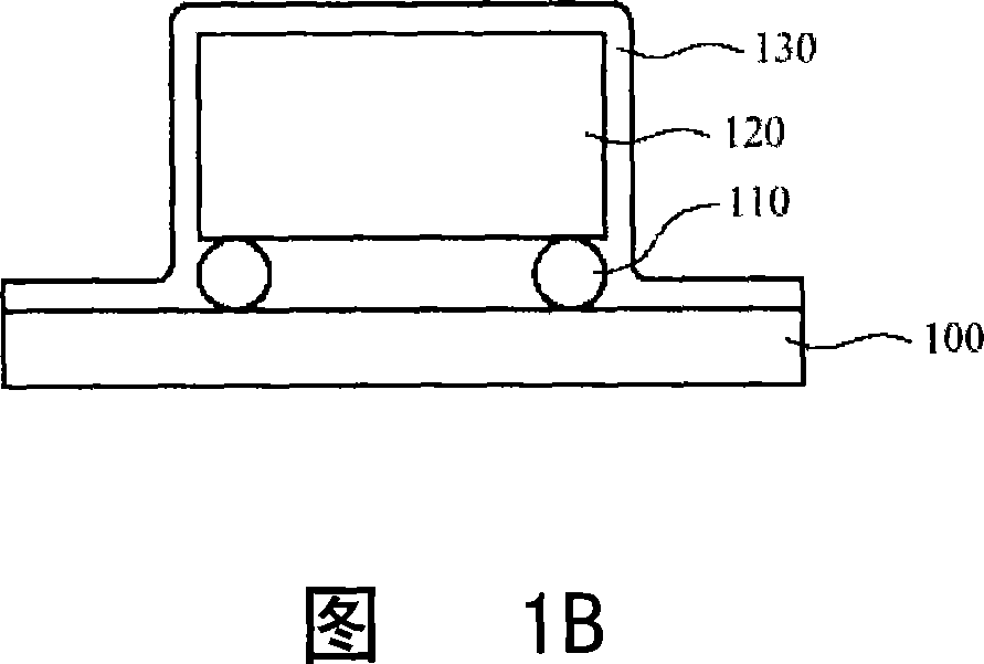
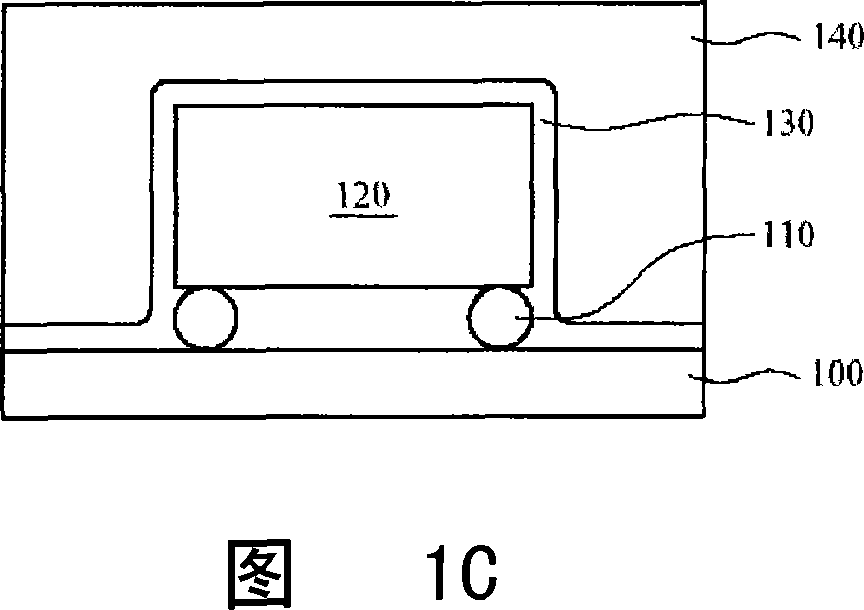
[0015] Please refer to FIG. 1A to FIG. 1C , which are schematic cross-sectional views of the manufacturing process of the LED packaging structure according to a preferred embodiment of the present invention. First, as shown in FIG. 1A , an LED chip 120 is provided, the refractive index of which is between 2.3 and 4. Referring to FIG. In this embodiment, a gallium nitride (GaN) light-emitting element is used, and its refractive index is 2.5. The anode electrode and the cathode electrode (not shown) on the light emitting diode chip 120 are electrically connected to a substrate having multiple contacts, such as the circuit board 100, through the metal bump 110 in a flip-chip manner; another option Yes, the LED chip 120 can also be electrically connected to the circuit board 100 by wire bonding. Next, as shown in FIG. 1B , a plasma chemical vapor deposition layer 130 is conformally formed on the LED chip 120 , wherein the refractive index of the plasma chemical vapor deposition l...


PUM


Abstract

A LED package structure is disclosed. The LED package structure includes a substrate, a light emitting diode, a plasma chemical vapor deposition layer and a transparent material layer, wherein the substrate has a plurality of contacts. The light emitting diode is disposed on the substrate and electrically contacted to the contacts. The plasma chemical vapor deposition layer is disposed on the light emitting diode and the refractive index of the plasma chemical vapor deposition layer is smaller than that of the light emitting diode. The transparent material layer is disposed on the plasma chemical vapor deposition layer and the refractive index of the transparent material layer is smaller than that of the plasma chemical vapor deposition layer.

Description

technical field [0001] The invention relates to a packaging structure of a light-emitting diode, in particular to a packaging structure of a light-emitting diode capable of improving light extraction efficiency. Background technique [0002] A light-emitting diode (LED) is a solid-state semiconductor device. The refractive index of its substrate is about 2.3 or a value close to 2.3. Generally, the packaging structure of a light-emitting diode uses a light-emitting diode chip (LED Chip) with a refractive index of about 2.5. The P pole and N pole are connected to the base material by wire bond or flip chip (Flip chip), and then covered with a transparent encapsulation resin with a refractive index of about 1.58. Due to the large difference in the refractive index of the base material (about 2.5) and the refractive index of the packaged transparent resin (about 1.58) in the package structure of this light-emitting diode chip, the light extraction efficiency is about 5%, and mos...

Claims


Application Information

Patent Timeline
Patent Type & Authority Applications(China)
IPC IPC(8): H01L33/00H01L25/075H01L21/50H01L33/44H01L33/56
CPCH01L2224/16225H01L33/44H01L33/56
Inventor 胡振宇蔡升颖王亲民
Owner CHI LIN OPTOELECTRONICS CO LTD
Why Eureka
Try Eureka