Method for removing etching residue

A technology for etching residues and functional layers, which can be used in microlithography exposure equipment, electrical components, semiconductor/solid-state device manufacturing, etc., and can solve problems such as difficulty and difficulty in removing photoresist

Inactive Publication Date: 2007-10-31
SEMICON MFG INT (SHANGHAI) CORP +1
View PDF1 Cites 27 Cited by
  • Summary
  • Abstract
  • Description
  • Claims
  • Application Information

AI Technical Summary

Problems solved by technology

varying degrees of difficulty depending on previous crafting
High temperature hard bakes, plasma etch residues and polymers, and crusts from ion implantation can make photoresist removal difficult

Method used


Image

  • Method for removing etching residue
  • Method for removing etching residue
  • Method for removing etching residue

Examples


Embodiment Construction

[0039] In order to make the above objects, features and advantages of the present invention more comprehensible, specific implementations of the present invention will be described in detail below in conjunction with the accompanying drawings.

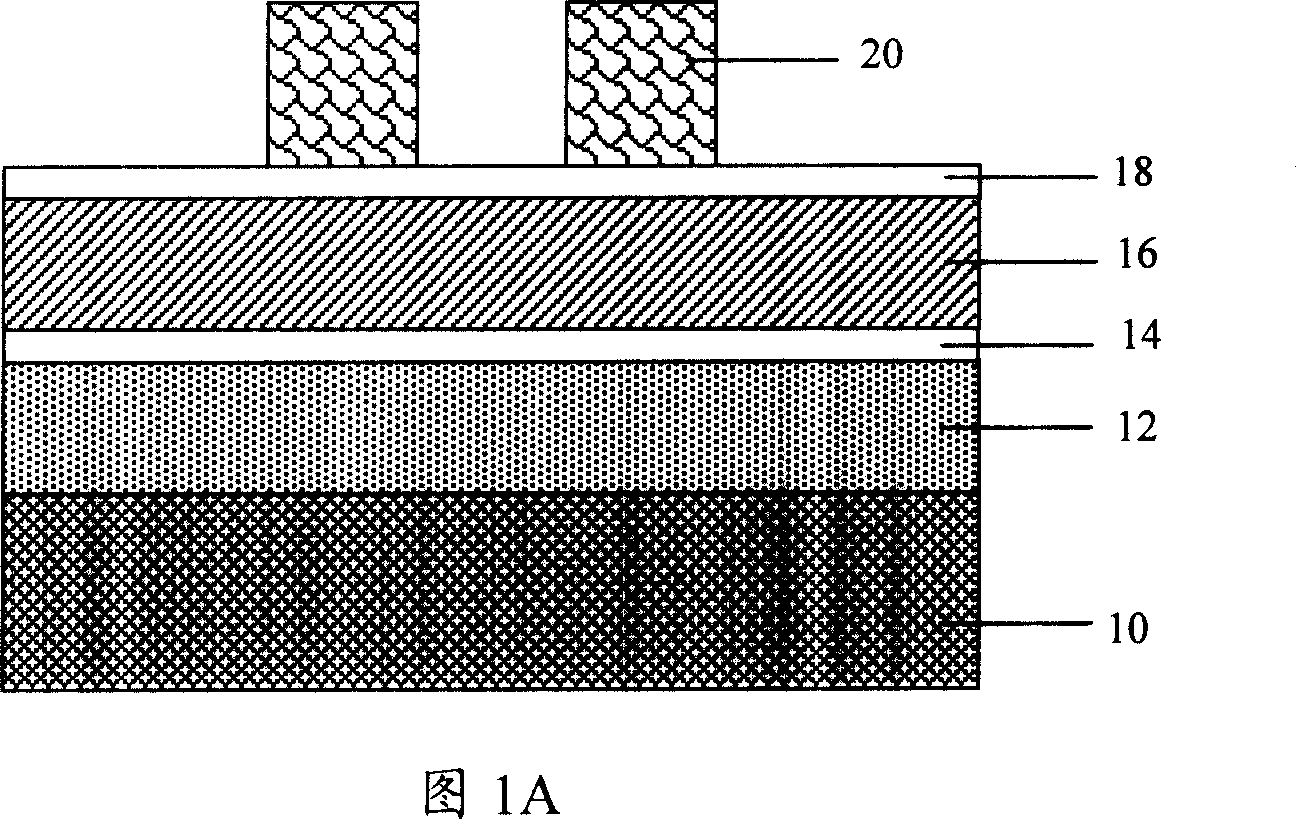
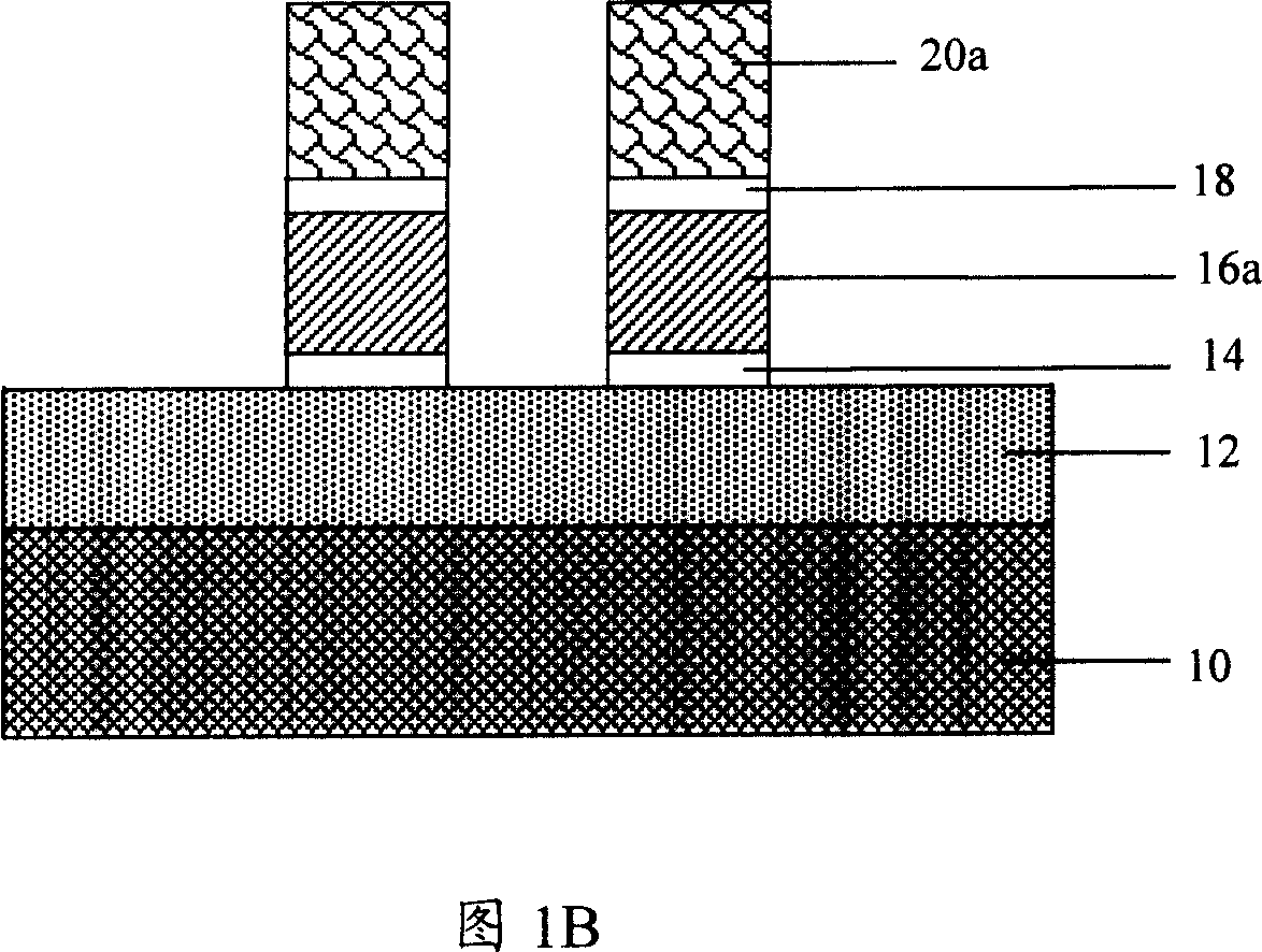
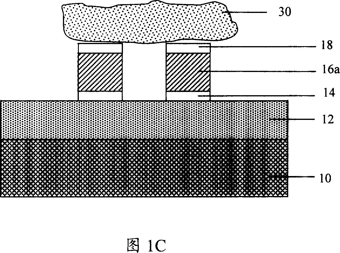
[0040]The method for removing etching residues of the present invention can be widely applied to the photoresist removal process after the etching process of many different metal or non-metal layer materials in the semiconductor manufacturing process. Here, the present invention illustrates the method of the present invention through preferred embodiments, and those of ordinary skill in the art should know that many steps can be changed, and the deposits produced by the metal layer material and the reaction can also be replaced. These general replacements Undoubtedly, it does not depart from the spirit and protection scope of the present invention.

[0041] The first embodiment of the method for removing photoresist residues after etch...


PUM


Abstract

This invention discloses one method to remove etch resides, which comprises the following steps: providing one semiconductor underlay; forming function layer on underlay and forming mask film layer on function layer; patterning the mask film layer; etching the said function layer to form needed image and to adopt gas spray to remove etch resides; removing etch resides. This invention method is to etch function layer to form needed image and then to remove etch resides and then adopts grey method to remove etch resides for final clear.

Description

technical field [0001] The invention relates to the technical field of semiconductor manufacturing, in particular to a method for removing photoresist residual substances after an etching process. Background technique [0002] The photolithography process is one of the most frequently used and most critical technologies in chip manufacturing technology. For semiconductor components, optoelectronic devices, etc., it is necessary to use the photolithography process to transfer the mask patterns of the basic components and circuits of the required components to On the photoresist pattern on the surface of the substrate, such as a wafer or a glass substrate. Usually, the basic process of photolithography includes three steps: glue coating, exposure and development. The purpose of the coating process is to create a thin, uniform, and defect-free photoresist film on the wafer surface. Exposure is to transfer the pattern on the mask to the photoresist coating by exposing lamps or...

Claims


Application Information

Patent Timeline
Patent Type & Authority Applications(China)
IPC IPC(8): G03F7/20G03F7/42H01L21/311
Inventor 王灵玲宋铭峰郭佳衢李建茹方标刘轩王秀郑莲晃王润顺
Owner SEMICON MFG INT (SHANGHAI) CORP
Why Eureka
Try Eureka