

Method of manufacturing semiconductor device
A manufacturing method and semiconductor technology, applied in the fields of semiconductor/solid-state device manufacturing, semiconductor devices, electric solid-state devices, etc., can solve the problems of complex bipolar transistor structure, a lot of time, and complex manufacturing process.
- Summary
- Abstract
- Description
- Claims
- Application Information
AI Technical Summary
Problems solved by technology
Method used
Image

Examples
Embodiment Construction
[0015] The preferred embodiments of the present invention will be described in detail below with reference to the drawings.
[0016] First, FIG. 1 will be briefly described.
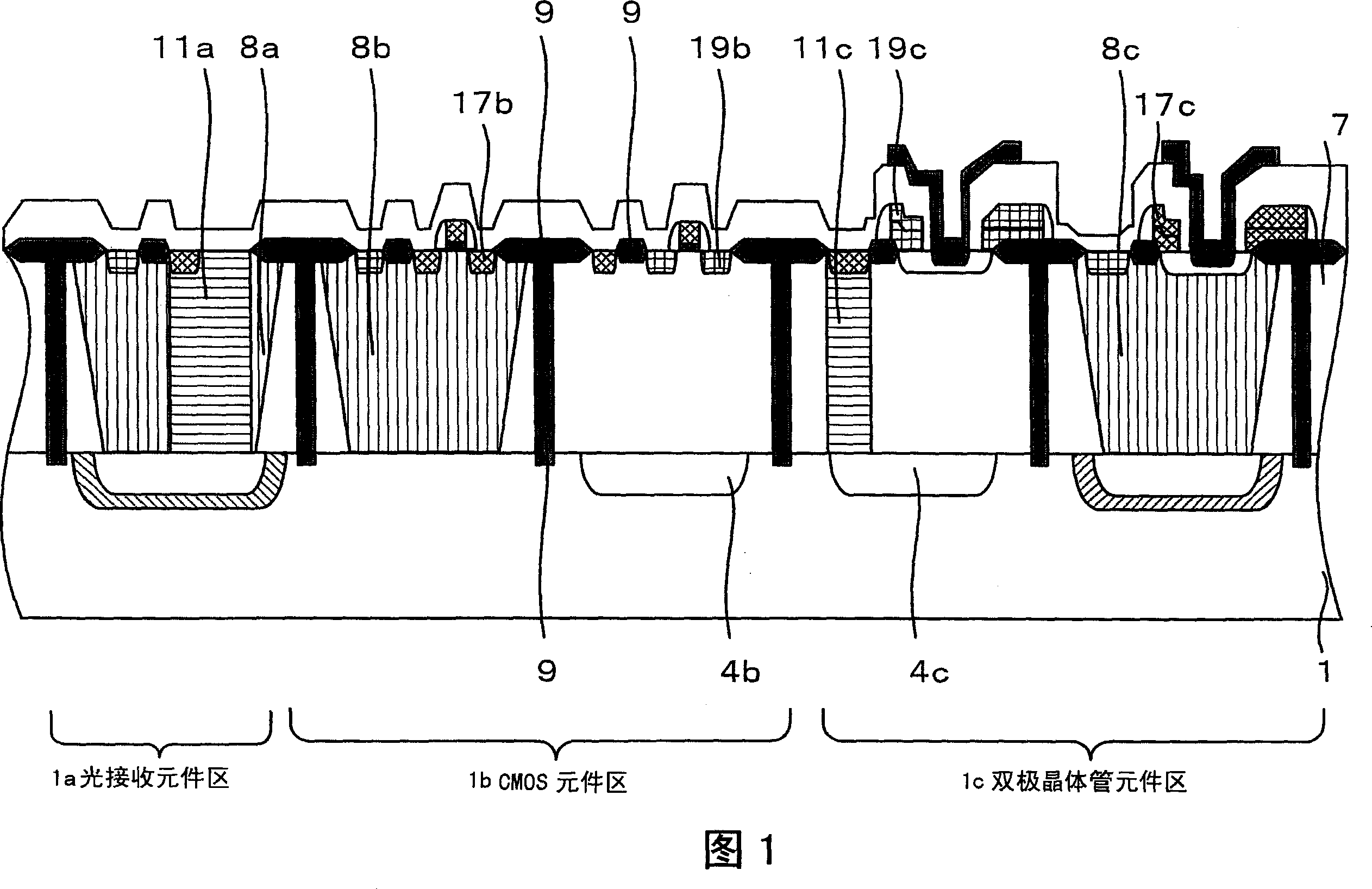
[0017] 1 is a schematic cross-sectional view of a semiconductor device in which a light receiving element part, a CMOS element, and a bipolar transistor element having a double-layer polysilicon structure are formed on one chip.
[0018] The outline of the manufacturing method of the above-mentioned semiconductor device will be described below.
[0019] As shown in FIG. 1, the light receiving element region 1a, the CMOS element region 1b, and the bipolar transistor region 1c are provided on the semiconductor substrate 1.
[0020] First, the same N-type ion implantation is performed to simultaneously form high-concentration N-type diffusion layers 4b and 4c in the CMOS element region 1b and the bipolar transistor element region 1c of the semiconductor substrate 1.
[0021] Next, an epitaxial layer 7 is formed...
PUM
 Abstract
Description
Claims
Application Information