Apparatus and method for arranging predetermined element on target platform

A target and platform technology, applied in the structural field of detecting and improving component placement accuracy, can solve problems such as monitoring chips, and achieve the effects of improving placement accuracy, reducing rework, and improving productivity

Active Publication Date: 2008-02-06
温泰克工业有限公司
View PDF0 Cites 27 Cited by
  • Summary
  • Abstract
  • Description
  • Claims
  • Application Information

AI Technical Summary

Problems solved by technology

However, there is no easy way for the user or manufacturer to monitor whether the chip is properly seated in the socket or whether the chip is making good contact with the socket in the socket

Method used


Image

  • Apparatus and method for arranging predetermined element on target platform
  • Apparatus and method for arranging predetermined element on target platform
  • Apparatus and method for arranging predetermined element on target platform

Examples


Embodiment Construction

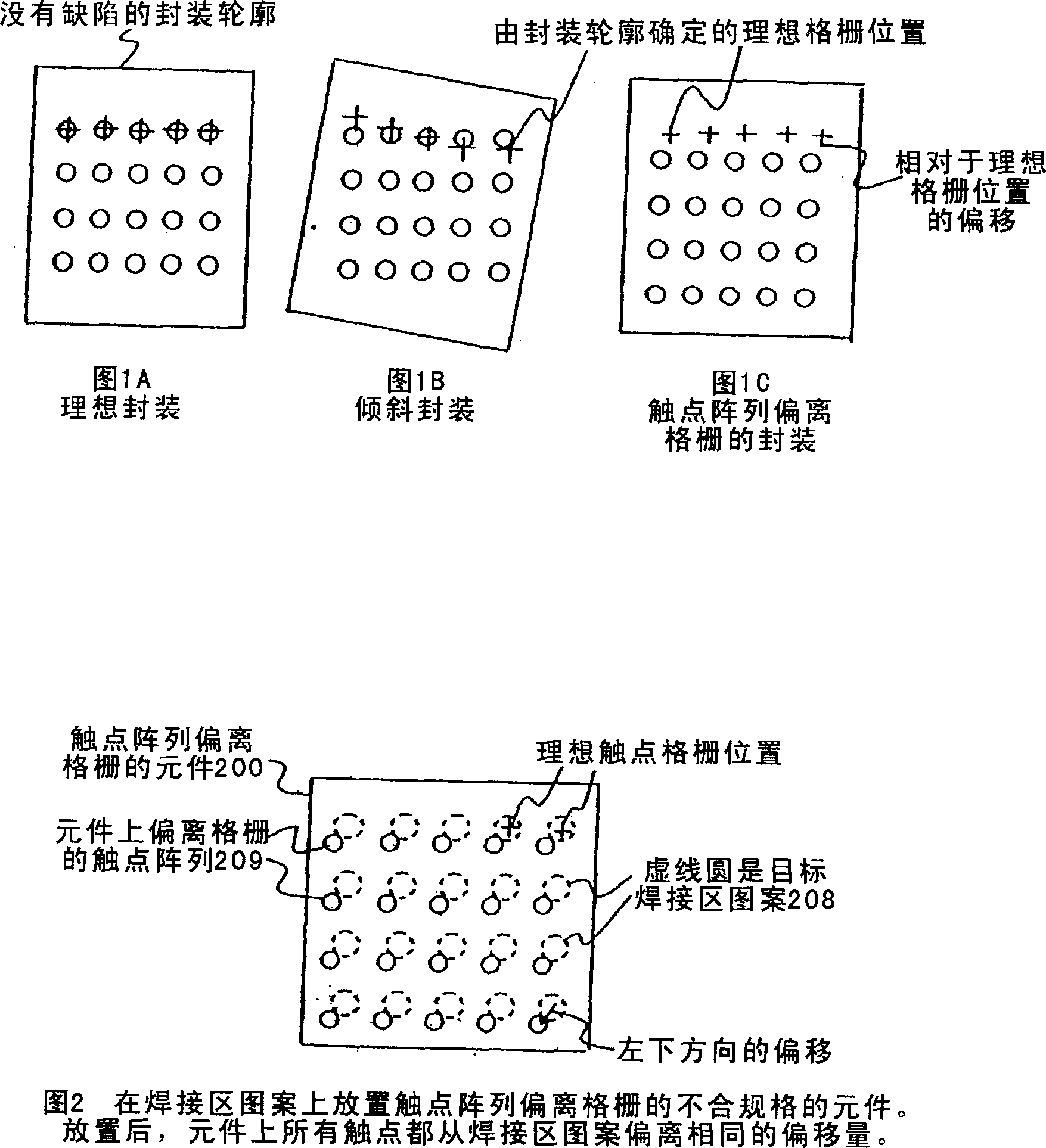
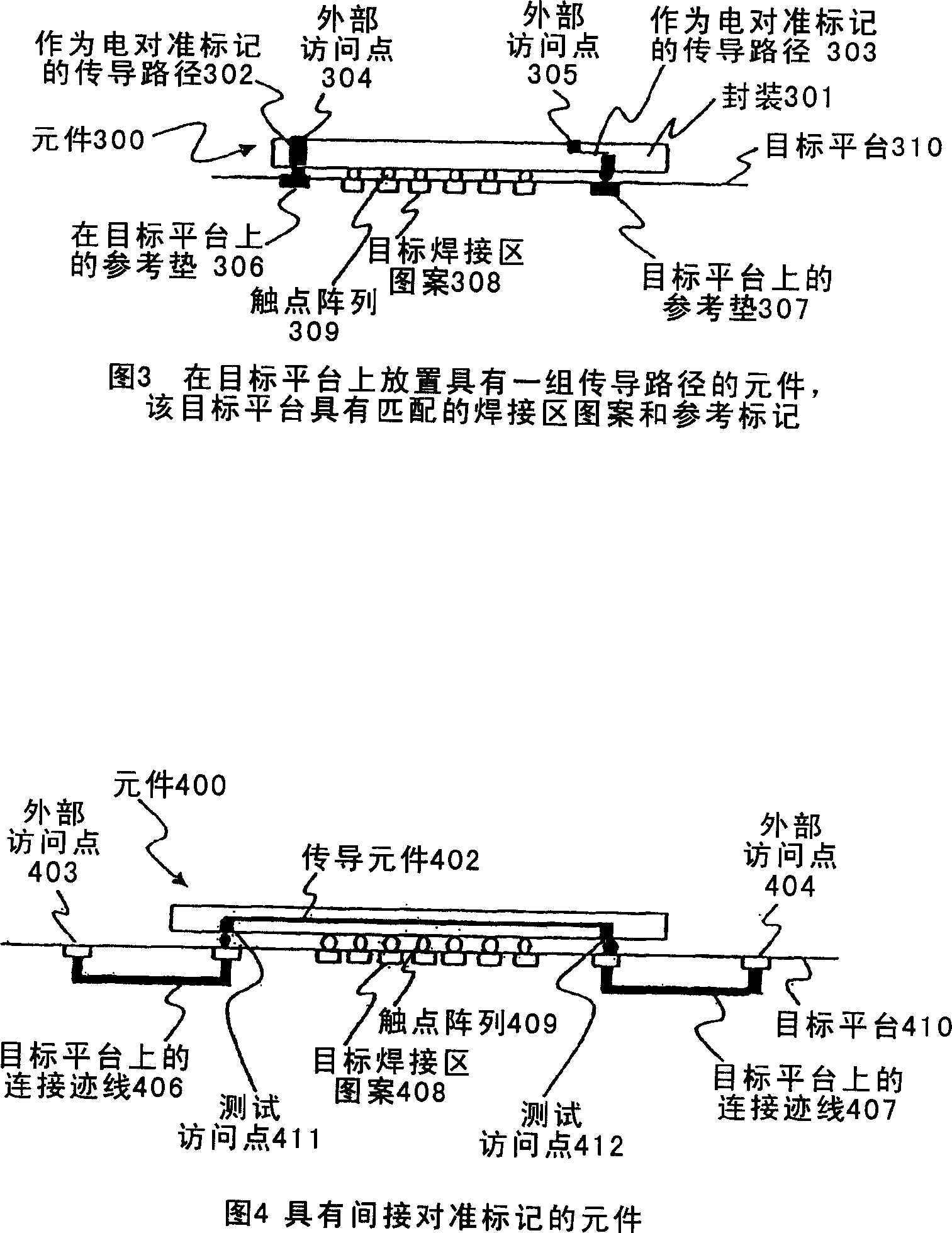
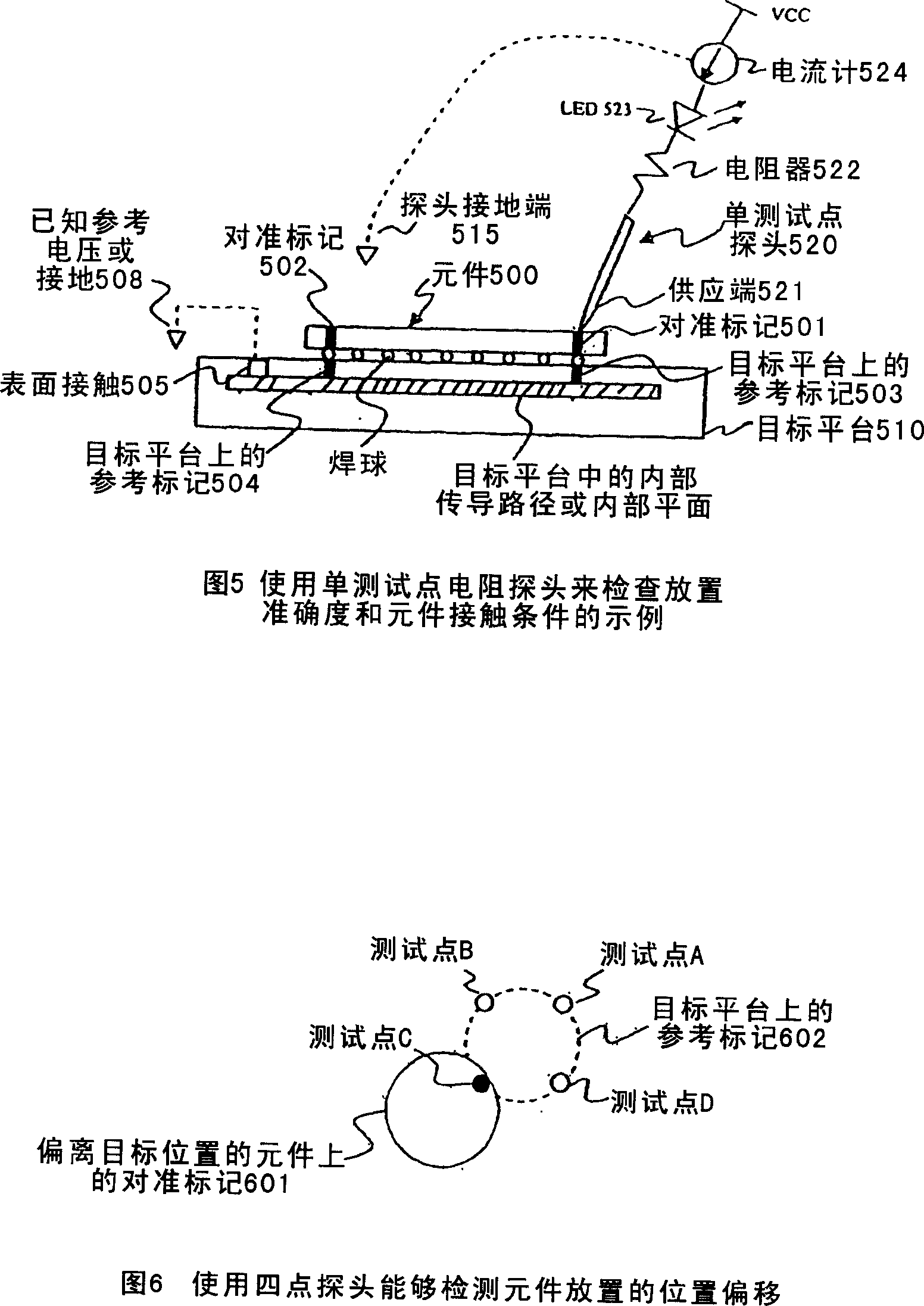
[0042] According to the present invention, alignment and probing techniques are described that improve the accuracy of component placement in assembly. More specifically, the present invention includes structures and methods for detecting and improving component placement accuracy on a target platform by incorporating alignment marks onto the component and reference marks onto the target platform using various probing techniques. A set of sensors in an array to form a multi-sensor probe capable of detecting deflection of a displacement element during assembly. Merely by way of example, the invention is applied to placing packaged devices on electronic substrates for electronic system fabrication. It should be realized, however, that the invention has broader applicability. Further details of the invention can be found throughout the specification of the invention, and in more detail below.

[0043] alignment mark

[0044] According to a preferred embodiment, the alignment ...


PUM


Abstract

The present invention relates to the assembling technique. According to the present invention, the present invention details the aligning and detecting techniques for placing precision of the improved components during assembling. Specifically, The present invention includes a method and a structure that are applied in all detection technologies to check and improve the position accuracy of the elements on the target platform by combining the elements with the aligning marks and the referential signs on the target platform. The sensor with a plurality of sensor probes can check the excursion of the excursion component when in assembling.

Description

technical field [0001] The present invention relates generally to assembly techniques, and more particularly to detecting and improving component placement accuracy on target platforms by incorporating alignment marks onto the components and reference marks onto the target platform using various probing techniques Degree structure and methods. Background technique [0002] Electronic devices have evolved over the years. As integrated circuits (ICs) increase in complexity and speed of operation, it is not uncommon for the number of devices to have pin counts in excess of a few hundred or even a thousand to increase. For example, high-speed designs require more power and ground pins. Such differential pairs are replacing single-ended signals at the device's input and output pins (I / O) to meet signal integrity requirements. In addition, as systems-on-chips become a reality, more and more pins are added to device I / O to support more functions. Taken together, many if not all...

Claims


Application Information

Patent Timeline
Patent Type & Authority Applications(China)
IPC IPC(8): H01L23/544H01L23/02H01L23/48H01L21/60H01L21/66H01L21/68H05K13/04H05K13/08
CPCH01L2224/16225
Inventor 孔-琛·陈
Owner 温泰克工业有限公司
Why Eureka
Try Eureka