Thickness reduced multi-chip stacking and packaging construction

A multi-chip, wafer technology, applied in electrical components, electrical solid devices, circuits, etc., can solve the problems of peeling and separation, general products have no structure, poor adhesion of electroplating layers, etc., and achieve the effect of improving support.

Inactive Publication Date: 2008-02-27
CHIPMOS TECH INC
View PDF0 Cites 2 Cited by
  • Summary
  • Abstract
  • Description
  • Claims
  • Application Information

AI Technical Summary

Problems solved by technology

Therefore, the back side of the first chip 220 faces the back side of the second chip 230, and the lead frame needs to be turned over when electrically connecting to form the bonding wires 251 and 252, and the upper and lower surfaces of the pins 212 must form a double-sided plating layer 213, resulting in an increase in the cost of the lead frame and package
In addition, since the sealant 240 is not well bonded to the general electroplating layer, if the double-sided plating layer 213 covers an excessively large area, the interface between the sealant 240 and the pins 212 will be peeled off easily.
[0005] It can be seen that the above-mentioned existing multi-chip stacked package structure obviously still has inconvenience and defects in structure and use, and needs to be further improved urgently.
In order to solve the above-mentioned problems, the relevant manufacturers have tried their best to find a solution, but no suitable design has been developed for a long time, and the general products do not have a suitable structure to solve the above-mentioned problems. This is obviously related. The problem that the industry is eager to solve

Method used


Image

  • Thickness reduced multi-chip stacking and packaging construction
  • Thickness reduced multi-chip stacking and packaging construction
  • Thickness reduced multi-chip stacking and packaging construction

Examples


no. 1 Embodiment

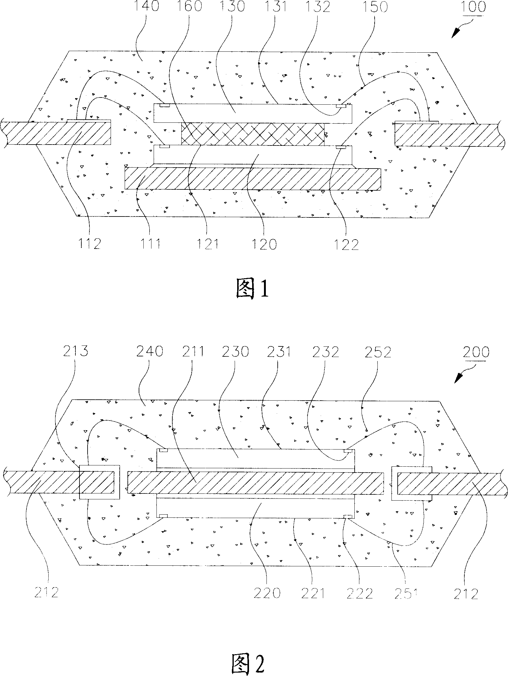
[0067] Please refer to FIG. 3 , which is a schematic cross-sectional view of a multi-chip stack package structure according to the first embodiment of the present invention. In the first embodiment of the present invention, a multi-die stacked package structure 300 mainly includes a spacer pad 311 (spacer pad) of a leadframe, a plurality of pins 312, a first chip 320, a first Two wafers 330 and a package of colloid 340 .

[0068] The spacer seat 311 and the pins 312 are cut from the same lead frame, and are made of metal, such as copper, iron or their alloys. Usually, the shape of the spacing seat 311 is like a traditional die pad or chip paddle, but the size may be slightly smaller.

[0069] The first chip 320 has a first active surface 321 and a first back surface 322 , and a plurality of first electrodes 323 (as shown in FIG. 4 ) are formed on the first active surface 321 . The first electrodes 323 can be electrically connected to some of the pins 312 by a plurality of fi...

no. 2 Embodiment

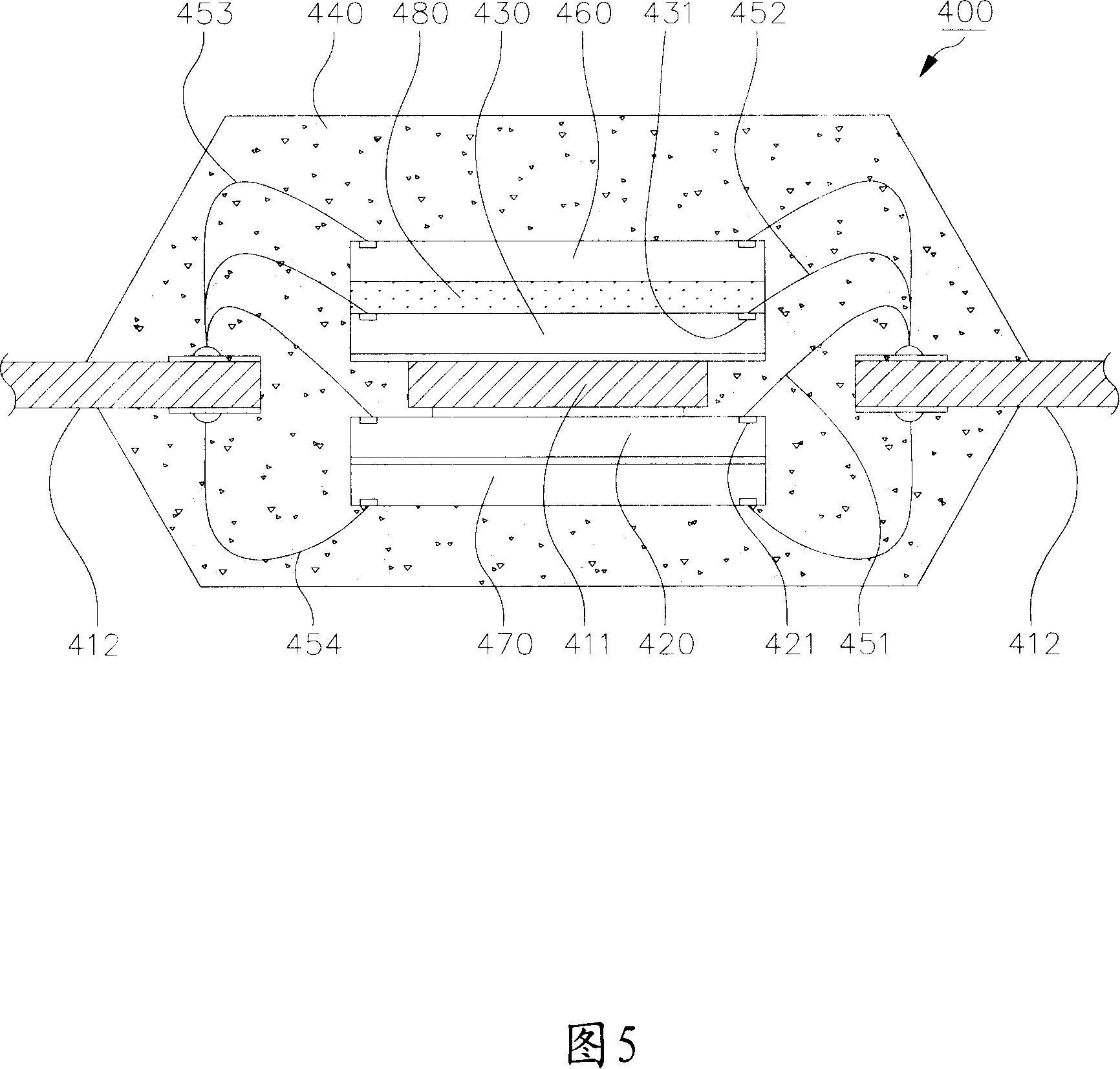
[0079] Please refer to FIG. 5 , which is a schematic cross-sectional view of another multi-chip stack package structure according to the second embodiment of the present invention. The invention is not limited to the number of sealed wafers. Another multi-chip stack package structure 400 disclosed in the second embodiment of the present invention, in addition to including a spacer seat 411 of a lead frame and a plurality of pins 412, a first chip 420, a second chip 430 and The encapsulant 440 has substantially the same components as the first embodiment, and further includes a third chip 460 and / or a fourth chip 470 and so on.

[0080] A plurality of first electrodes 421 are formed on the active surface of the first chip 420 , and are electrically connected to some of the pins 412 by a plurality of first bonding wires 451 .

[0081]A plurality of second electrodes 431 are formed on the active surface of the second chip 430 , and are electrically connected to some of the pins ...


PUM


Abstract

The present invention relates to thickness-reduced-multi-wafer-stacked package, and mainly includes an interval substrate and even numbers of pins of a line frame, a first wafer, a second wafer and a sealing colloid. Even numbers of first electrodes are formed on active surface of the first wafer, and are electric connected to parts of the pins. Even numbers of second electrodes are formed on active surface of the second wafer, and are electric connected to parts of the pins. The sealing colloid is used for combining the interval substrate, the pins, the first and the second wafers. In specific, the active surface of the first wafer clings down to the interval substrate, and the active surface of the second wafer clings up to the interval substrate. The first pins of the first wafer are not covered by the interval substrate, thus thickness of multi-wafer-forward stack can be reduced.

Description

technical field [0001] The present invention relates to a semiconductor chip stack package structure, in particular to a reduced thickness multi-chip stack package structure using a lead frame. Background technique [0002] In a multi-chip package structure (Multi-Chip Package, MCP), stacking a plurality of chips vertically to save package size is a fairly mature technology. However, spacers between the dies increase the overall package thickness. [0003] Please refer to FIG. 1 , which is a schematic cross-sectional view of a conventional multi-chip stack package structure. The existing conventional multi-chip package structure 100 utilizes a lead frame as a chip carrier, and includes a chip holder 111 and a plurality of pins 112, a first chip 120, a second chip 130 and a package with a lead frame. Colloid 140. The first wafer 120 and the second wafer 130 are stacked on the wafer holder 111 in a forward direction. The plurality of bonding wires 150 electrically connect ...

Claims


Application Information

Patent Timeline
Patent Type & Authority Applications(China)
IPC IPC(8): H01L25/00H01L23/488
CPCH01L2224/48091H01L2224/48247H01L2224/4826H01L2224/73215H01L2224/73265
Inventor 林鸿村
Owner CHIPMOS TECH INC
Why Eureka
Try Eureka