

Optical transducer packaging structure and optical sensing module
A light-sensing module and packaging structure technology, applied in radiation control devices, TVs, color TV components, etc., can solve the problems of glue material flowing to the surface of light-sensing chips, high packaging accuracy requirements, and difficulty in manufacturing. , to avoid overflow to the surface of the light sensor chip, the production yield and quality are stable, and the area and volume are reduced.
- Summary
- Abstract
- Description
- Claims
- Application Information
AI Technical Summary
Problems solved by technology
Method used
Image

Examples
Embodiment Construction
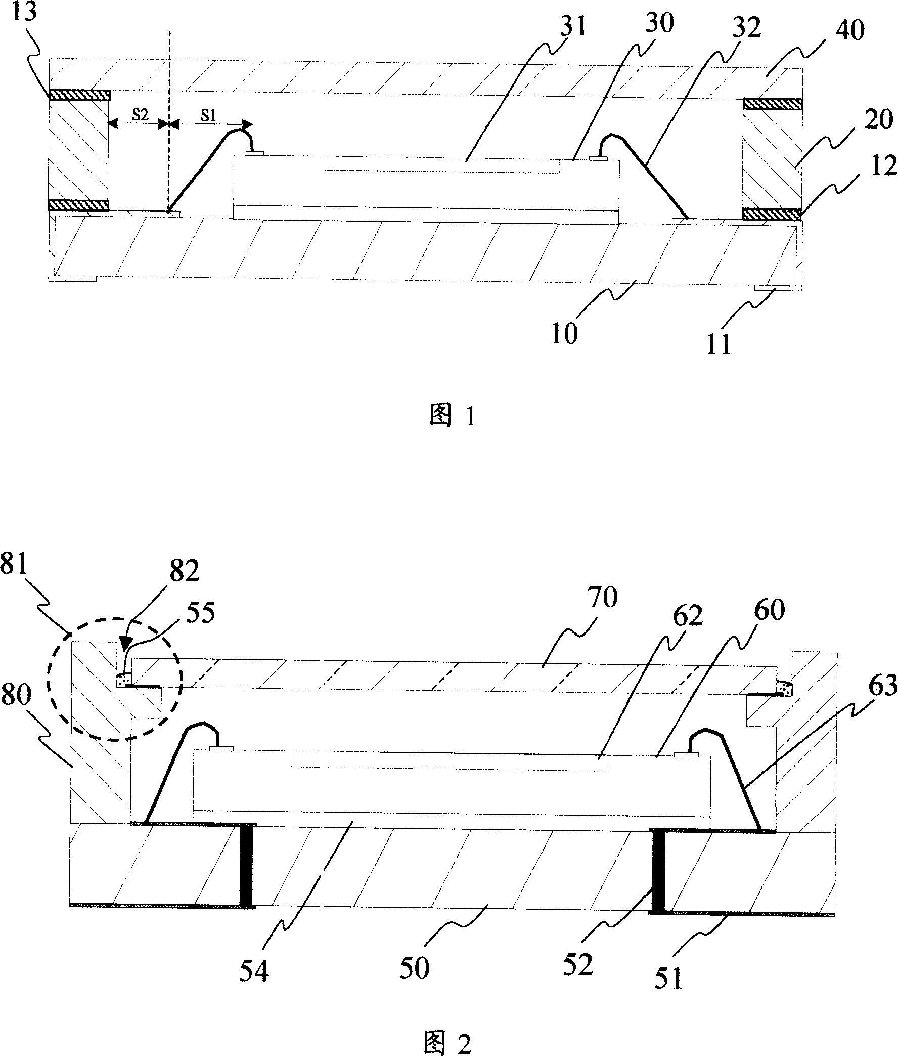
[0033] As shown in FIG. 2 , it is a schematic diagram of the package structure of the light sensor provided by the embodiment of the present invention. The light sensor packaging structure is mainly composed of a substrate 50 , a light sensing chip 60 , a frame 80 and a transparent layer 70 .
[0034] Wherein, the material of the substrate 50 can be BT (Bismaleimide Triazine) resin, FR5 resin or ceramic material, and several metal wirings 51 are arranged on the upper surface and the lower surface of the substrate 50, and these metal wirings 51 are plated through holes passing through the substrate 50. 52 are electrically connected. The light-sensing chip 60 is adhered to the upper surface of the substrate 50 through the adhesive layer 54, and has a light-sensing area 62 on its surface, and is connected to the metal wiring 51 with the metal wire 72 through the wire bonding method, and is formed with the substrate 50. electrical connection. The light-transmitting layer 70 is a...
PUM
 Abstract
Description
Claims
Application Information