Vertical BJT, manufacturing method thereof

A region and collector technology, applied in the field of vertical BJT and its manufacturing, can solve problems such as the best current gain of vertical BJT devices

Inactive Publication Date: 2008-02-27
DONGBU HITEK CO LTD
View PDF0 Cites 9 Cited by
  • Summary
  • Abstract
  • Description
  • Claims
  • Application Information

AI Technical Summary

Problems solved by technology

Since the thickness and width of a single base layer are determined by the manufacturing process, the best current gain of the vertical BJT device cannot be obtained through the CMOS process

Method used


Image

  • Vertical BJT, manufacturing method thereof
  • Vertical BJT, manufacturing method thereof
  • Vertical BJT, manufacturing method thereof

Examples


Embodiment Construction

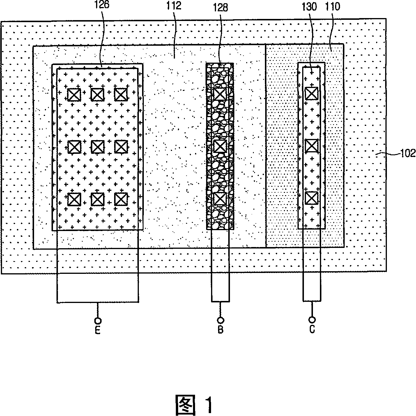
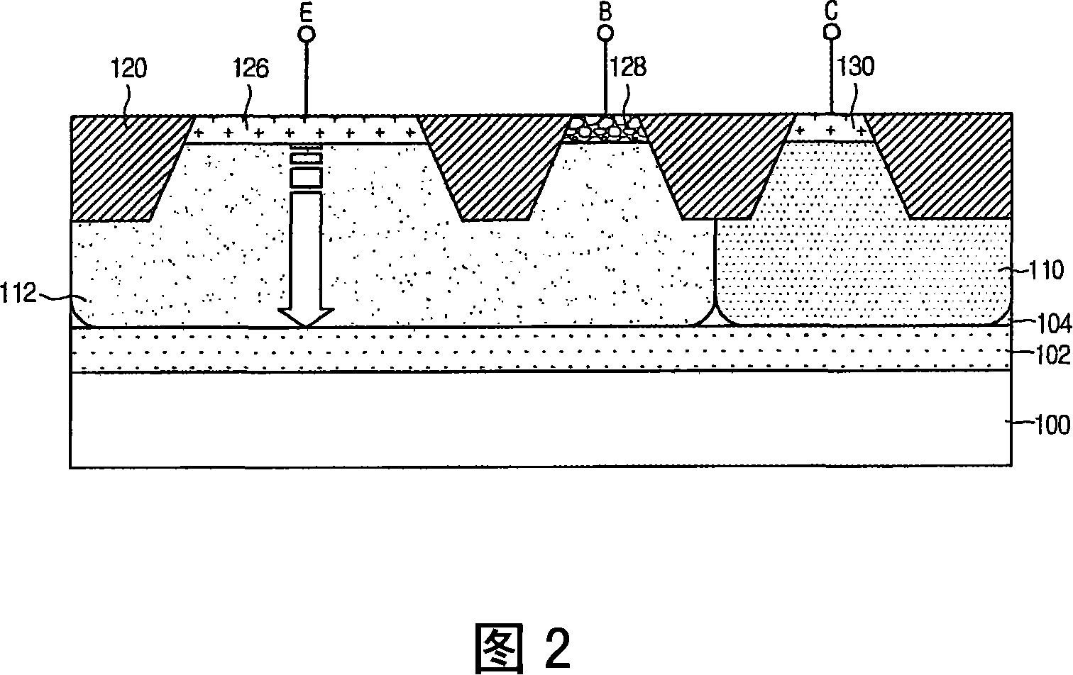
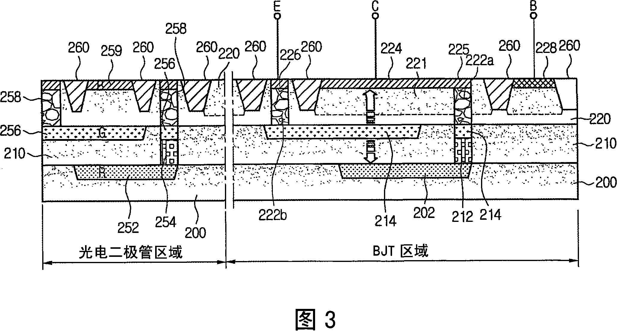
[0013] As shown in FIG. 3 , in the photodiode region, a red photodiode region 252 is formed in the first epitaxial layer 200 formed over the semiconductor substrate. The second epitaxial layer 210 is grown, and the second P-type epitaxial layer 210 is formed by implanting P-type ions into the second epitaxial layer 210 . The first plug 254 is formed by implanting high-concentration ions into the second P-type epitaxial layer 210 to connect the second P-type epitaxial layer 210 to the red photodiode region 252 for sending signals.

[0014] After forming a photoresist layer pattern on the second P-type epitaxial layer 210, a green photodiode region 256 is formed in the second P-type epitaxial layer 210 by partially implanting ions into the second P-type epitaxial layer 210. , grow a third epitaxial layer 220 on the second P-type epitaxial layer 210 including the green photodiode region 256 , and form an STI region 260 in the third epitaxial layer 220 to define an active region. ...


PUM


Abstract

A vertical BJT with maximum current gain in the photodiode region and its manufacturing method, the vertical BJT includes first and second collector regions located in different epitaxial layers; an emitter region inserted in the first and second collector regions Between; a base region formed on the first collector region and the emitter region, and the second collector region and the emitter region. According to an embodiment, since a BJT may be formed together with a photodiode, and a collector current flows up and down based on a double base structure, the magnitude of current may be increased.

Description

technical field [0001] The present invention relates to a vertical BJT (bipolar junction transistor) and its manufacturing method. Background technique [0002] Generally, an image sensor is a semiconductor device that converts an optical image into an electrical signal. The image sensor may be a charge-coupled device (CCD) image sensor in which individual metal-oxide-semiconductor (MOS) capacitors are placed in close proximity to allow charge carriers to charge or discharge charge carriers from the capacitor. A Complementary Metal Oxide Semiconductor (CMOS) image sensor continuously detects an output by providing MOS transistors corresponding to the number of pixels using a switching mode. CMOS technology can integrate peripheral devices such as control circuits and signal processing circuits into the sensor. A CMOS image sensor may include a photodiode and a MOS transistor in each unit pixel to detect signals in a switching mode and form an image. [0003] According to ...

Claims


Application Information

Patent Timeline
Patent Type & Authority Applications(China)
IPC IPC(8): H01L29/732H01L27/146H01L21/331H01L21/822
CPCH01L29/66272H01L27/14643H01L27/0664H01L29/732H01L29/0821H01L27/146
Inventor 林秀
Owner DONGBU HITEK CO LTD
Why Eureka
Try Eureka