Chip welding spot on-line detecting, defect identification device and chip packaging device

A chip and defect technology, applied in the field of chip solder joint inspection, can solve problems such as unfavorable chip real-time inspection and system integration, and achieve the effect of low price and high degree of automation

Inactive Publication Date: 2008-03-05
SUN YAT SEN UNIV
View PDF0 Cites 44 Cited by
  • Summary
  • Abstract
  • Description
  • Claims
  • Application Information

AI Technical Summary

Problems solved by technology

However, this existing method is often used in thermal performance testing and rework processes in flip-chip soldering and BGA packages to improve process control and reduce rework costs during rework. It is not conducive to large-scale real-time chip detection and system integration.

Method used


Image

  • Chip welding spot on-line detecting, defect identification device and chip packaging device
  • Chip welding spot on-line detecting, defect identification device and chip packaging device

Examples


Embodiment Construction

[0028] The present invention will be further described below in conjunction with the accompanying drawings.

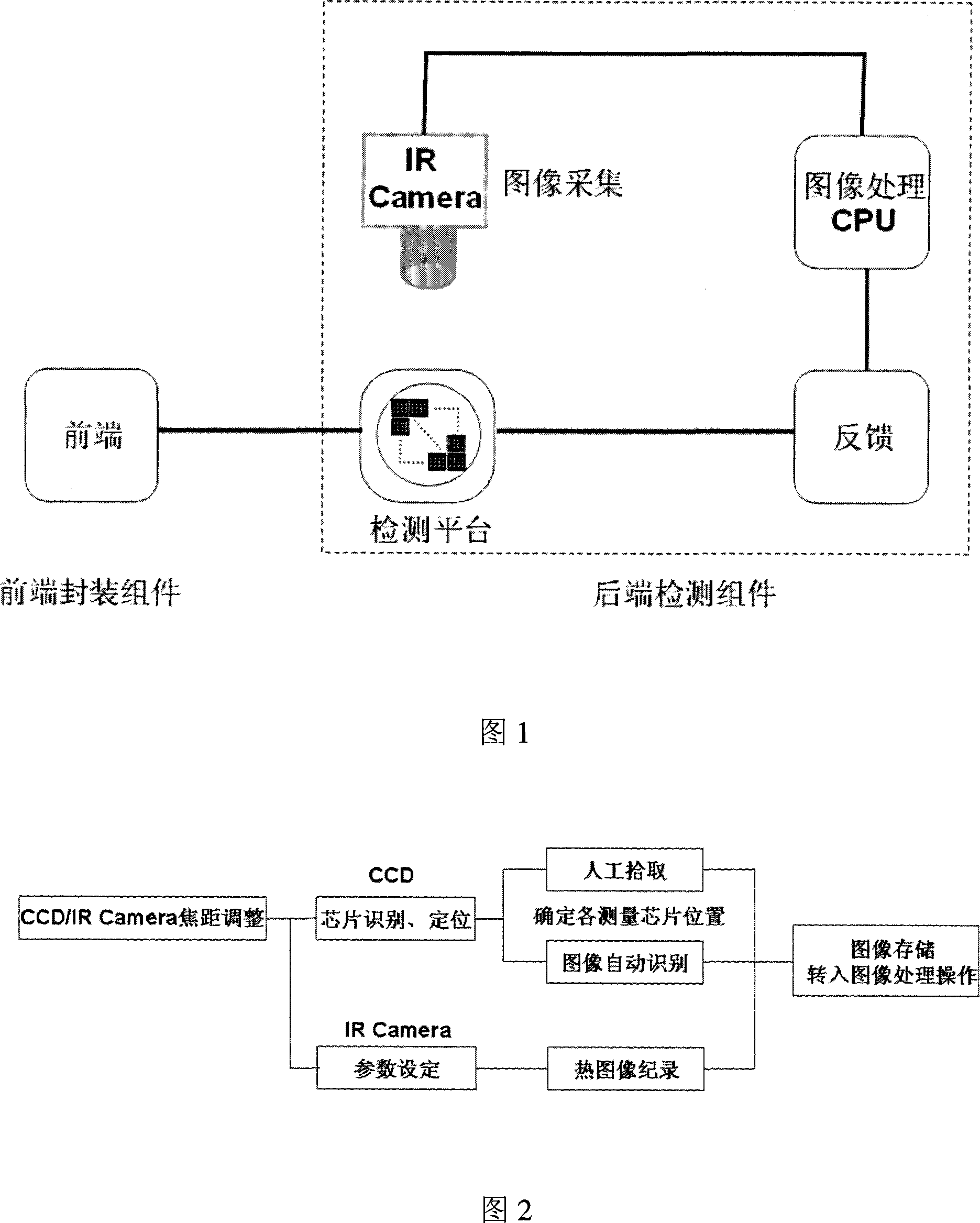
[0029] The structure diagram of the online detection and defect identification equipment of the present invention is shown in Figure 1. It is composed of a front-end interface, a detection platform, an image acquisition device, an image processing system and a feedback device; the front-end interface serves as a connection bridge with the front-end packaging components , The solder joint inspection platform components are integrated with the front-end packaging components through the front-end interface; the inspection platform is responsible for processing the chip samples transmitted from the front-end; the image acquisition device includes CCD image acquisition and IR Camera infrared thermal imaging system, CCD image acquisition system for chip For positioning and automatic measurement, the IR Camera infrared thermal imager collects the surface temperature of the chip s...


PUM


Abstract

This invention provides an on-line test for chip solder joints and a package device including a test platform, an image collecting device, an image processing device and a front interface, in which, said platform for processing chips and testing samples is connected with the chip package device via the front interface and is capable of heating the sample, said image collecting device is set above the platform and set with an infrared thermal imaging system to pick up thermal images of the sample, said image process system includes a central processor for processing the thermal images of the sample picked up by the collecting image to judge solder joints of the sample.

Description

Technical field [0001] The invention relates to the detection of chip solder joints and chip packaging technology. technical background [0002] Integrated circuits (such as IC components), electronics (such as HEMT components) and optoelectronics (such as LED components) components need to be packaged on the shell, this kind of packaging or directly glued to the shell with silver glue or other glue , Or use eutectic welding, flip-chip welding (welding surface or solder bump) and other solder directly on the shell. The bonding surface not only plays the role of fixing the chip, but also serves as an electrical interconnection channel and heat transfer channel between the chip and the outside. Therefore, the quality of the bonding surface will seriously affect the performance of the packaged device. Due to the actual process or operation and other reasons, the bonding surface often has defects such as voids, bubbles, and delamination. In order to ensure the quality stability and r...

Claims


Application Information

Patent Timeline
Patent Type & Authority Applications(China)
IPC IPC(8): H01L21/66H01L21/50H01L21/60G01N25/72
Inventor 王钢范冰丰
Owner SUN YAT SEN UNIV
Why Eureka
Try Eureka