Liquid crystal display device with thin-film transistor on color film and its manufacture method

A thin-film transistor and liquid crystal display technology, which is applied in semiconductor/solid-state device manufacturing, instruments, electrical components, etc., can solve the problems of light transmittance and aperture ratio decrease, and light-transmitting materials do not further increase the transmittance, etc., to achieve improved Transmittance, eliminate poor light leakage and other defects, improve the effect of product yield

Active Publication Date: 2008-03-26
BEIJING BOE OPTOELECTRONCIS TECH CO LTD +1
View PDF1 Cites 33 Cited by
  • Summary
  • Abstract
  • Description
  • Claims
  • Application Information

AI Technical Summary

Problems solved by technology

The TFT LCD device with this structure overcomes the unfavorable factors caused by the alignment accuracy, but it still has the following disadvantages: the coated light-transmitting material does not further improve the transmittance; it needs 5 photolithography processes to manufacture thin-film transistors; the gate insulating film and The passivation protective film covers the color filter layer, resulting in a decrease in light transmittance and aperture ratio

Method used


Image

  • Liquid crystal display device with thin-film transistor on color film and its manufacture method
  • Liquid crystal display device with thin-film transistor on color film and its manufacture method
  • Liquid crystal display device with thin-film transistor on color film and its manufacture method

Examples


Embodiment Construction

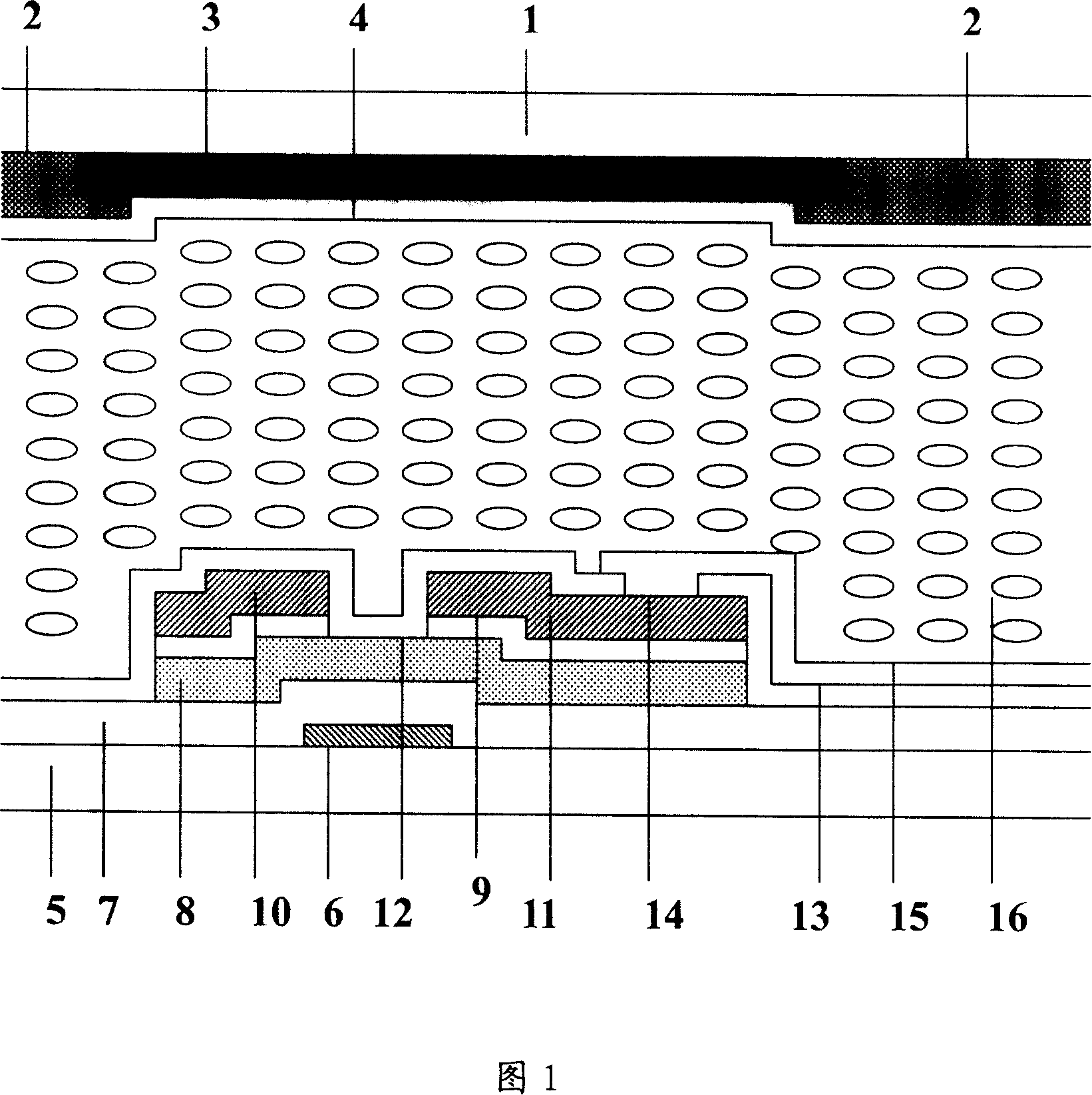
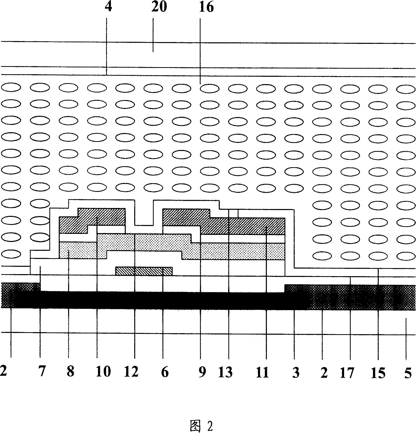
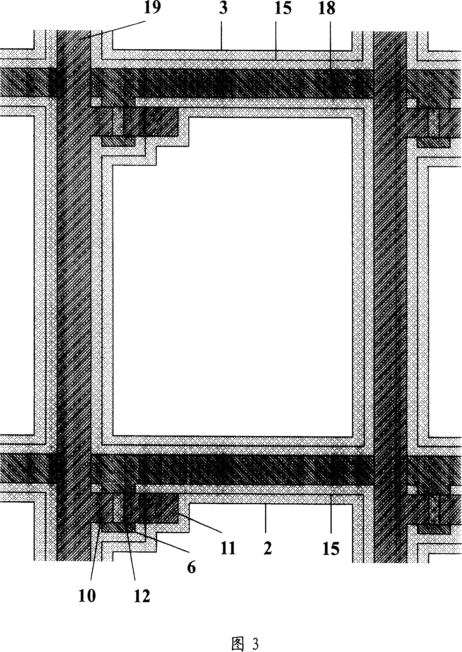
[0049] Specific embodiments of the present invention will be described in detail below in conjunction with the accompanying drawings. It should be pointed out that the thickness and area size of each layer of films and materials in the drawings do not reflect the real proportion of the device structure, but are only for clearly illustrating the content of the present invention.

[0050] The liquid crystal display device of the present invention comprises an array substrate and a common electrode substrate, liquid crystal molecules sandwiched between them, peripheral circuits and driving circuit boards, and a backlight source. The difference from traditional liquid crystal display devices is that the color filter layer and black matrix are formed on the glass of the array substrate, and the thin film transistor is formed on the color filter composed of the color filter layer and black matrix; the other glass substrate is only transparent Common electrode made of conductive film...


PUM

PropertyMeasurementUnit
thicknessaaaaaaaaaa
thicknessaaaaaaaaaa
thicknessaaaaaaaaaa

Abstract

This invention discloses a sort of liquid crystal display that the thin film is above the chromatic film, and it consists of the nether baseboard, the black matrix which is formed under the nether baseboard, the chromatic filter layer which is formed in the hatch of the black matrix and corresponds to the picture element area, the over protective film which is formed above the chromatic filter layer and the black matrix, the grating line and the grating pole which is formed above the over protective film, the thin film transistor which is formed in the grating pole, the data wire and the power pole and the leakage pole are formed above the thin film transistor, the deactivation protective layer which is formed above the area of the leakage and the other exceptant part of the picture element area, the picture element pole which is formed above the picture element area and the over protective film, and it contacts with the part of the leakage pole, the upper baseboard, the common electric pole which is formed above the upper baseboard, the liquid crystal molecular layer which is formed between the upper baseboard and the nether baseboard. This invention advances the penetrant rate and the hatch rate of the liquid crystal display, and it predigests the technique.

Description

technical field [0001] The invention relates to a liquid crystal display device and a manufacturing method thereof, in particular to a liquid crystal display device with a thin film transistor on a color filter and a manufacturing method thereof. Background technique [0002] Due to the advantages of thinness and low power consumption, flat panel displays are widely used in portable displays. Among various flat panel displays, liquid crystal display devices have been widely used in computer monitors, notebook computers and televisions due to their advantages of high definition and picture quality. The image display of liquid crystal display is realized by utilizing the optical anisotropy and polarization characteristics of liquid crystal molecules. These characteristics of the liquid crystal molecules themselves cause their different alignments to change the refraction and transmission of incident light. Because of the anisotropic dielectric properties of liquid crystal mo...

Claims


Application Information

Patent Timeline
Patent Type & Authority Applications(China)
IPC IPC(8): G02F1/1362G02F1/1335G02F1/1333G03F7/20H01L21/00
Inventor 龙春平
Owner BEIJING BOE OPTOELECTRONCIS TECH CO LTD
Why Eureka
Try Eureka