Supercharge Your Innovation With Domain-Expert AI Agents!

Conveying calibration device and wafer transmission system using the same

A technology of a wafer transfer system and a calibration device, which is applied in the directions of transportation and packaging, conveyor objects, furnaces, etc., can solve the problems of inability to define the position of the wafer notch, increase the damage of the wafer edge, and the complicated transfer process, so as to improve the production transfer. Efficiency, accurate calibration, and the effect of simplifying system equipment

Active Publication Date: 2010-05-12
BEIJING NAURA MICROELECTRONICS EQUIP CO LTD
View PDF6 Cites 2 Cited by
  • Summary
  • Abstract
  • Description
  • Claims
  • Application Information

AI Technical Summary

Problems solved by technology

However, due to the mechanical clamping of the edge of the wafer, and the wafer is thin and brittle, the possibility of damage to the edge of the wafer due to force is increased during the clamping process, which reduces reliability
[0012] Each of the above three methods has its own advantages and disadvantages, all of which have a certain impact on the reliability of wafer transmission. Moreover, they have a common disadvantage, that is, they cannot correct the calibration of wafer eccentricity and wafer notch. Definition of position. Therefore, wafer aligners must be installed in the entire transport system in all three methods, and the target wafer must be sent to the wafer aligner for calibration before the atmospheric / vacuum manipulator transports the wafer into the process reaction chamber for semiconductor processing , definition, making the transmission process too complicated.

Method used


Image

  • Conveying calibration device and wafer transmission system using the same
  • Conveying calibration device and wafer transmission system using the same
  • Conveying calibration device and wafer transmission system using the same

Examples


Embodiment Construction

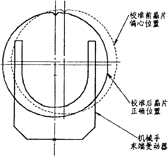
[0051] A preferred embodiment of the handling and calibrating device of the present invention is as follows: Figure 8As shown, including the end effector, the rear end of the end effector is connected with the mechanical arm 5, and the front end is provided with a picker for grabbing objects. The rear end of the end effector is hinged with the mechanical arm 5, according to Other connection methods can also be used if necessary.

[0052] There are two end effectors, respectively the first end effector 1 and the second end effector 3, the rear ends of the first end effector 1 and the second end effector 3 are respectively It is hinged with the mechanical arm 5 and can rotate around the hinge point independently; the front end is respectively connected with the first object fetcher 2 and the second object fetcher 4 .

[0053] Such as Figure 9 As shown, the first object fetcher 2 and the second object fetcher 4 are respectively provided with an object retrieval groove 8, and ...


PUM


Abstract

The present invention discloses a transportation calibration device and a crystal wafer transmission system applying the same, comprising a terminal effector, wherein, the back end of the terminal effector is articulated with a manipulator, and the front end of the terminal effector is provided with a fetching device used to grab objects; the present invention also comprises a driving device whichcan drive the terminal effector to rotate around an articulated point and a calibration device used to position and calibrate a grabbed object; a fetching groove is arranged on the fetching device; the lower part of the fetching groove is provided with a positioning plane used for the center positioning to the grabbed object; a calibrator is arranged on the manipulator, which is used to define the circumferential angle of the grabbed object. The present invention is mainly used for a crystal wafer transmission system in the manufacturing process of semiconductor crystal wafers to transmit andcalibrate the crystal wafers, is reliable in transportation, accurate in calibration, can be applied to both atmospheric environment and vacuum environment, cancels the transmission process of delivering the crystal wafers to the crystal wafer calibrator, reduces transmission path and time, improves the efficiency of production as well as transmission, and simplifies system equipment.

Description

technical field [0001] The invention relates to a semiconductor processing equipment, in particular to a transport calibration device and a wafer transmission system using the device. Background technique [0002] In the process of semiconductor processing, the wafer needs to be processed from the wafer chamber to the process reaction chamber. After the process is completed, the wafer is transferred back from the process reaction chamber to the wafer chamber. In the whole process, the atmospheric manipulator and the vacuum manipulator are the exercising parts and core components of the wafer transfer function, the central nerve of the wafer transfer system, and play the role of a transportation hub. [0003] Such as figure 1 Shown is the transfer process for wafers with a thickness of 200 mm or less; [0004] Such as figure 2 Shown is the transfer process for 300mm wafers. [0005] It can be seen that in every link of wafer transfer and handling, the atmospheric / vacuum ...

Claims


Application Information

Patent Timeline
Patent Type & Authority Patents(China)
IPC IPC(8): H01L21/677H01L21/68B65G47/90B65G49/07
Inventor 张之山
Owner BEIJING NAURA MICROELECTRONICS EQUIP CO LTD
Features
  • R&D
  • Intellectual Property
  • Life Sciences
  • Materials
  • Tech Scout
  • Unparalleled Data Quality
  • Higher Quality Content
  • 60% Fewer Hallucinations
Learn More