Large area reverse roller impression method for micro-structure of flexible base macroelectron manufacture

A microstructure and large-area technology, applied in the direction of microstructure technology, microstructure devices, chemical instruments and methods, etc., can solve problems such as stress concentration of flexible substrates and microstructures, damage to flexible substrates, complex processes, etc., to avoid additional processes , Eliminate film retention and reduce stress concentration

Inactive Publication Date: 2008-04-30
XI AN JIAOTONG UNIV
View PDF0 Cites 14 Cited by
  • Summary
  • Abstract
  • Description
  • Claims
  • Application Information

AI Technical Summary

Problems solved by technology

[0006] First, the imprinting method is essentially mechanical forced molding, which requires a large imprinting force, which is likely to cause stress concentration in the flexible base and microstructure;
[0007] Second, the imprinting method inevitably forms a certain thickness of "retained film" on the formed electronic material. In order to realize the function of the macroelectronic system, the "remained film" must be removed by additional process means, such as etching , chemical corrosion, ion milling, etc., the process of removing the "retained film" is extremely complicated, especially for large-area flexible base macro electronic systems, there is a problem of equipment applicability, it must be suitable for large-area removal of "retained film", Without damaging flexible substrates and functional 3D microstructures

Method used


Image

  • Large area reverse roller impression method for micro-structure of flexible base macroelectron manufacture
  • Large area reverse roller impression method for micro-structure of flexible base macroelectron manufacture

Examples


Embodiment Construction

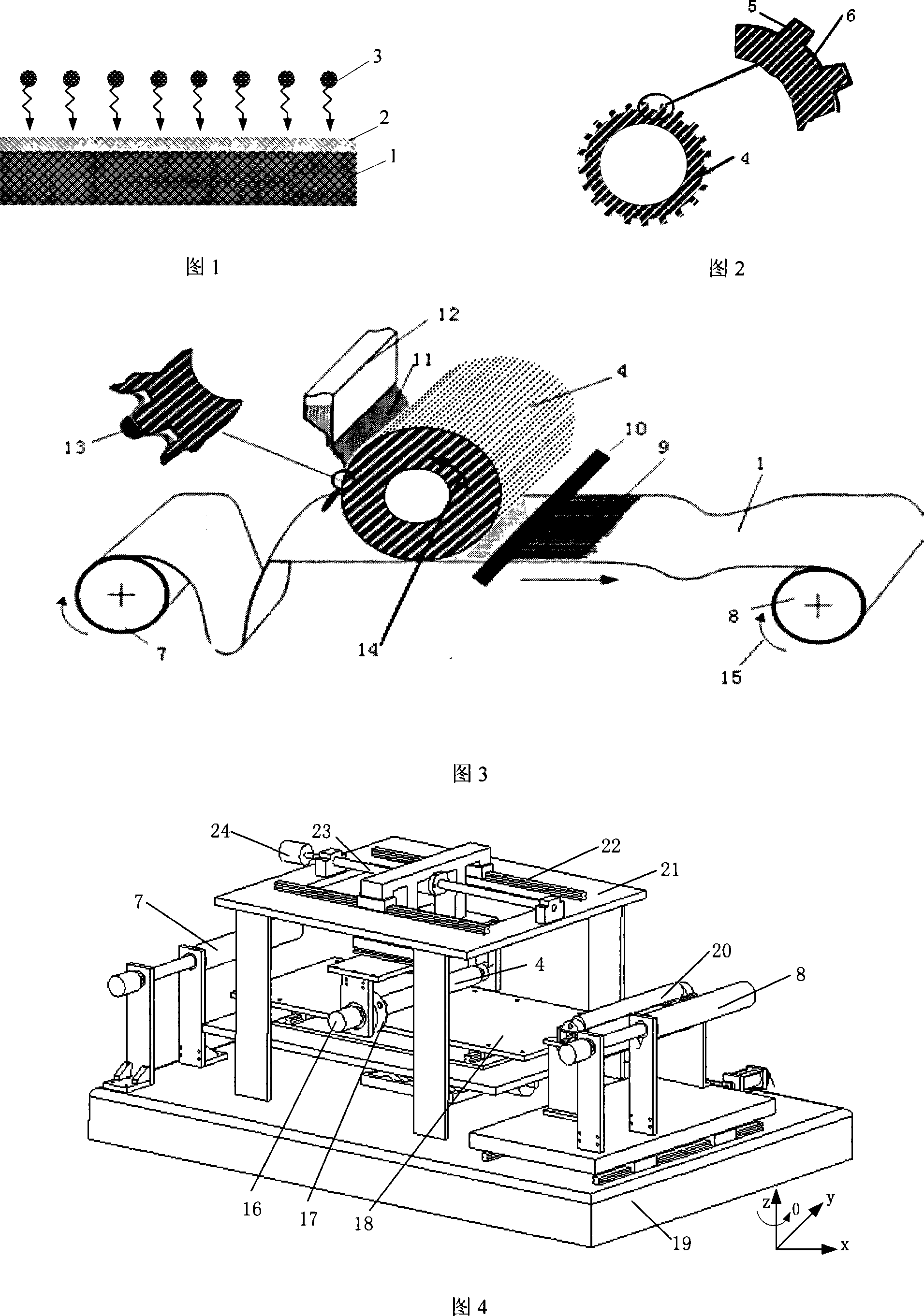
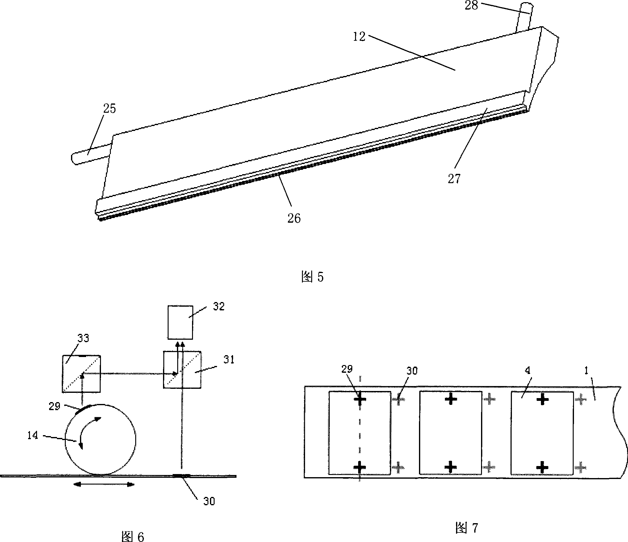
[0025] Referring to the accompanying drawings, Fig. 1 to Fig. 7 respectively show the flow chart of the large-area reverse embossing process of microstructures in the manufacture of flexible macroelectronics.

[0026] The basic working principle of the present invention is: coating the electronic material on the surface of the mold engraved with the microstructure, completing the patterning of the electronic material, and then transferring the patterned electronic material on the surface of the mold to the flexible substrate by continuous rolling. on the material. Add a photocuring agent to the electronic functional material, and use a cold ultraviolet light source for curing after reverse imprinting. The mold roller rotates at a constant speed while moving in translation, and the linear speed of the rotation matches the translation speed, so as to realize no friction between the microstructure on the mold and the microstructure to be replicated. When printing multilayer circ...


PUM


Abstract

The invention discloses a large-area reverse coil embossing shaping method for using flexible substrate and macro electron to produce middle micro structure. The invention uses reverse coil embossing technique, relative chromatograph aligning technique, and ultraviolet solidifying technique, to produce large-area three-dimension functional micro structure needed by macro electric appliance. The invention eliminates the left membrane in general embossing, to eliminate the additional process needed for treating left membrane. And the invention adds optical solidifier in electric functional material to solidify cold ultraviolet light source, thereby reducing the thermal deformation of flexible material. The invention has wide application in the productions of macro electron system as expandable large-size display, electric paper, OLED, film RFID, flexible solar sail, portable X-ray imager, portable radar, space solar power system, antenna device, and electromechanical intelligent cover adhered on the surface of arbitrary three-dimension structure.

Description

technical field [0001] The invention belongs to the technical field of micro-nano manufacturing, and in particular relates to a large-area reverse embossing method for three-dimensional functional microstructures in the manufacture of flexible macroelectronics (electronic devices based on thin film transistors (TFT). The method is mainly used in unrollable large-format displays, electronic paper, OLED, thin-film RFID, flexible solar sails, portable x-ray imagers, portable radars, flexible solar power supply systems and antenna devices, and electromechanical intelligence attached to the surface of any three-dimensional structure. Manufacture of macroelectronic systems such as skins. Background technique [0002] Electronic systems based on thin-film transistors (TFT: Thin-Film-Transitor) glass plate-based or flexible film-based electronic systems continue to tend to large-area integration (for example, a single side span of more than 1 meter), forming ...

Claims


Application Information

Patent Timeline
Patent Type & Authority Applications(China)
IPC IPC(8): B81C5/00H01L21/00H01L21/02H01L21/64B81C99/00
Inventor 刘红忠丁玉成蒋维涛兰红波张昭卢秉恒史永胜尹磊邵金友
Owner XI AN JIAOTONG UNIV
Why Eureka
Try Eureka